


One of the ways to build more complex, powerful, and cost-effective electronic systems is stacking chips on top of each other. Imec recently compared the two main options for going 3D: interposer-based stacking and 3D stacking. The goal of the exercise was to detect whether the stacking and packaging processes for the two options result in a different yield, and where in the processes those differences originate.
Chip stacking yield is a major cost indicator, so any improvement will directly relate to the stack’s profitability. The results revealed two instances of yield loss. During 3D stacking, there is a loss when the two chips are bonded with thermo-compression. This is due to the particular distribution of forces during the compression. And the interposer-based stacks show a known yield loss for the second chip, which is bonded later than the first. This can be prevented by adding a NiB (nickel-boron) capping layer to the interposer’s microbumps.
Building the test chips
The advantage of having both research, design, and processing in-house is that we can test all options by designing dedicated test chips, fabricated in-house. For this experiment, we built our 3D stacks starting from a 65nm CMOS test chip, which we call Package Test Chip version Q (PTCQ) (Figure 1).
The particular design of this chip allows us, among other things, to investigate the yield of the chip’s connections in the stack. Foremost, these are the microbump connections between two chips layers. But we also look at the package bumps: the connections of the 3D stack with the package and the outside world. In addition, the chip also contains heaters to investigate the thermo-mechanical behavior of stacks.
Testing the connection between stack layers is done through loop back structures. These are two points of contact that are interconnected on the chip. With 832 loopback structures covering the whole connected surface of the chip, we can then make a map of functional and blocked loopback structures at each stage in the process.
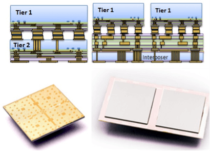
The two major ways of stacking chips that we tested are 3D stacking and interposer-based stacking (Figure 2). In the former, the dies are added on top of each other, building a tower of chips. In the latter die dies are stacked next to each other on an interposer, a common ground floor.
The test chip was made in two versions. One is to serve as top die of the stack, where it will sit face-down with its metal layers connected to the lower chip through microbumps. This PTCQ chip is 200µm thick and has CuNiSn microbumps with a diameter of 15µm. The second version will serve as bottom chip of the ‘3D stacked IC’ stack. Again, face down, its metal layer is connected to the outside world through Cu pads with 50 micrometer diameter. On its backside however, it is thinned down to 50 micrometer, revealing the through silicon vias (TSVs) that were etched through the chip’s body and that connect with the chip’s circuits. These TSVs are a mere 5µm wide and are crowned with Cu microbumps of 25µm diameter, making them ready to contact the 15µm microbumps of the upper chips.
In the interposer-based stack, this second version of the PTCQ test chip is replaced by the interposer chip. This chip is both larger (it will house several chips next to each other) and simpler (it just makes the TSV connections between the chips; it doesn’t need any transistors).
So in both stacks, the 15µm bumps of the top chip will have to be aligned and bonded to the 25µm bumps of the lower chip, with a 40µm pitch. The actual bonding is done through thermo-compression. The bonding force corresponds to a pressure of around 69MPa applied to the 37,000 microbumps of a test chip. The highest temperature reached is 270℃ 38 degrees above the melting point of Sn.
Comparing the yield
With these test chips ready, the yield exercise was started. The way we did this was to go through the whole process of fabricating 3D chip stacks, focusing on the 3D-enabling technologies: wafer thinning, thin-wafer handling, TSV and microbump processing, and stacking and packaging. At various stages in the processing, we measured the yield: the percentage of 3D chips that functions correctly. Where there were any differences, we tracked the possible causes.

Stacking a first test chip on the interposer resulted in a near 100% yield. But the yield of stacking a test chip on a second, thinned test chip is slightly lower. This was revealed by the test structures, where we did find some open loopback circuits at the corners and edges of the chip-on-chip stack.
There are two differences in the stacking process that can explain this difference. First, the thinned-down test chip is thinner (50µm) than the interposer (100µm). This makes it more flexible under the applied compression. Second, the layout of the copper pads that serve to connect the stacks to the package is different. In the thermo-compression process, these pads are the only contact with the tool. They translate the bonding force to the microbumps on the other side of the chip. But some of the microbumps at the edges and corners of the die fall outside the area where the larger copper pads are. As a result, these receive less force, especially with the thinner, more flexible die. So this leads to a number of microbumps that stay unconnected in the chip-on-chip package.
A second yield-loss effect was known beforehand: Stacking two dies on the interposer is done in two cycles. Without additional measures, the Cu microbumps on the landing site for the second die will oxidize during stacking of the first die. A way to overcome this is by plating NiB on the interposer microbumps before stacking. In our test, we measured the difference in yield between the ‘raw’ process and the one where we microbumps are plated. In the first case, there is a substantial yield loss, which is completely regained with the NiB plating.
Yield as a cost determinant
Yield, and more specifically the compounded yield of all stacking steps, is one of the most important factors determining the cost of 3D stacking. So determining and solving hidden yield problems in either stacking method will have a direct effect on the cost (and profitability). With this experiment we have shown how appropriately designed test chips can help to compare various stacking processes and to uncover sources of yield loss. ~imec


