
Imec did their usual stellar job of demonstrating what needs to happen in the semiconductor manufacturing world to enable the next generation of semiconductor devices and keep the industry moving forward to achieve 3nm integrated circuits (ICs). More importantly, however, they discussed how to use 3D in both packaging and transistor cell design to achieve system integration that will enable integrated circuits to eventually mimic the brain and bring the much-hyped artificial intelligence to reality.
Luc Van den hove, CEO, imec, kicked off the conference with a global view of the key issues facing mankind. While health topics were discussed in the morning sessions, Van den hove tackled hunger and pollution briefly in the afternoon. He said Europe plans to be carbon neutral by the year 2050, thus helping reduce pollution and the carbon footprint. Technology in general, and particularly ICs, will play key roles in helping to resolve some of these issues above.
3D Saves Energy
However, before the electronics industry comes to the world’s rescue, a few things need to be resolved with regard to energy usage. Solving the world’s problems generates a considerable amount of data that must be analyzed to develop possible solutions. The energy required to process, and store one Zettabyte of data uses the equivalent amount of energy as approximately 180,000,000 homes. This would suggest that technology is exacerbating the carbon neutrality problem rather than solve it in the near term. However, by continuing to scale semiconductor technology and to develop new 3D packaging technologies, ICs can help to move the world a bit closer to carbon neutrality as these system integration solutions will reduce the amount of energy needed to analyze the data.
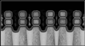
Van den hove summarized many of the programs imec is working on to reduce power consumption and improve IC performance. imec has been a key player in extreme ultraviolet (EUV) lithography development, which enables the industry to scale at a lower cost and lower power than optical lithography. The development of a high numerical aperture EUV tool will potentially enable single patterning at 3nm. This will help to drive the gate-all-around (GAA) transistors into manufacturing, as shown in Figure 1. Samsung, an imec partner, has recently announced their first iteration of GAA transistors for production sometime in the future.
AI Drives 3D Growth
The other imec speakers at ITF USA then filled in the gaps, albeit more along the lines of semiconductor manufacturing technology.
Arnaud Furnemont discussed scaling. “2D scaling stops because of device physics, 3D scaling stops because of economics,” he explained. That message would seem to be good news for the semiconductor industry, as the economics driving artificial intelligence (AI) seem to be much greater than those that were driving the PC and smartphone industry.
If Furnemont’s statement holds true, the industry should be in for a good long run of 3D growth. 3DNAND and DRAM continue to move vertically with NAND approaching 128 layers. Hynix now refers to their NAND product as 4D, because of the peripherals placed under the memory stack, thus shrinking the die size.
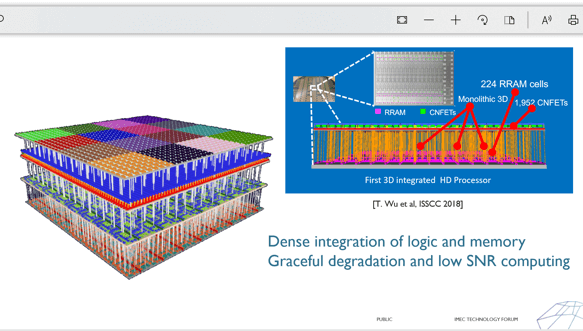
Systems-on-chip (SoCs) are reaching their limits not only in die size but also in effectiveness due to long interconnect layouts. Furnemont suggested smart partitioning of the logic using through-silicon vias (TSVs) to connect vanilla CMOS to SRAM. This method could also be used to connect the core logic to any memory in an attempt to create a 3D AI chip or a neuromorphic computing device. Furnemont also touched on 3D packaging, and indirectly chiplets, which is currently a hot topic for system integration in the IC industry.
Furnemont also addressed the performance-versus-power challenge that is facing the industry. At the moment there does not appear to be a clear solution, but he challenged the audience to continue working on the problem collaboratively to develop a solution.
Scaling Up!
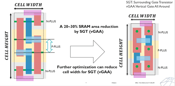
Nato Horiguchi then discussed CMOS scaling and how vertical scaling would continue to extend CMOS technology. The surrounding gate transistor (SGT) or GAA as used by others will be enabled by EUV lithography which has finally moved from development to production. Horiguchi demonstrated the advantages of the vertical devices IMEC is working on where the source-drain is put inside the gate, which then leads to a smaller cell area. Vertical SRAM can be combined with horizontal logic in a system technology co-optimization process to develop the optimum CMOS device (FIgure 2). This creative scaling supports Furnemont’s earlier message of 3D scaling getting the industry to at least 3nm, and possibly smaller.
3D System Integration
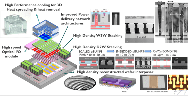
Eric Beyne then discussed 3D system integration and the impact packaging and system technology co-optimization will have in creating systems-in-package (SiP) solutions, where now the end user can pick and choose the best of breed memory, CPU, power chip, communication silicon, and package it together to create an optimized electronics system, as opposed to trying to design and build an SoC, which may need to have tradeoffs in the circuity as a result of the manufacturing process.
When the industry achieves the ultimate goal of multiple silicon to silicon chips bonded together using TSVs, it will be possible to build some very powerful systems that have better performance and power properties than an SoC.
Achieving silicon-to-silicon bonding is not without its challenges. Beyne led the audience through IMEC’s road map from 2.5D, which is in production today, to 3D which is still several years away. Challenges such as heat removal, via-to-contact alignment, and design all must be solved to successfully build a 3D SoC. The industry has been working on TSV silicon-to-silicon technology for SoC since the mid 2000’s. Based upon the presentations there are still a few more years to go before these systems are in mainstream production.
Computing at the Edge
Jan Rabaey presented on the cognitive edge, and the fact that the rapid increase in data, 50 Zettabyte’s in 2019 to 2000 Zb in 2024 will create challenges with analysis as the world is moving from the internet of Things (IoT), to the Internet of Actions (IoA), where we will need to be able to take action on the data that has been created. This happens to be one of the key challenges to implementing AI with the IoT. The analysis and interpretation of the data drive the success of the application. Rabaey went on to discuss the computational-based learning landscape.

- Bayesian machine learning
- Deep neural networks
- Neuromorphic computing
- High dimensional computing SDM holographic.
Each has different IC requirements as well as programming requirements, and each manages data differently. This adds to the challenges in developing the different AI systems that are moving into the market place.
The good news for semiconductor design and manufacturing is that it will require 3D integration to meet the system learning challenges, and it will not be one size fits all. As has already been demonstrated, an IC for AI can range from a 32-bit MCU in a doorbell trained to identify 6-10 faces and thus enable entry to the house, to a highly sophisticated GPU running both analytics and machine learning in an autonomous vehicle.
Interconnect Scaling
Zsolt Toke wrapped up the afternoon with one of the key issues facing the industry as it scales to 3nm: Interconnect scaling. As copper vias shrink, the resistance increases, thus increasing the heat in the interconnect. Reducing dielectric capacitance can help, but finding a metal combination with lower resistance seems to be the optimal solution at the moment, as the industry has nearly squeezed all the capacitance out of the dielectric. (To digress, in a discussion with another former CVD engineer we lamented that if the industry had understood that airgaps were a positive thing 20+ years ago, we would have had fewer gray hair!)
Toke commented that back-end-of-line (BEOL) scaling requires EUV insertion, new conductors and scaling boosters. Toke proposed a potential metal pitch of 16nm which could be achievable with EUV. However, at 16nm there are challenges with variability, mechanical stability, and process complexity. Toke proposed a semi-damascene process to help with the challenges.
New metals or metal combinations could also help to lower the resistance in the interconnect. Toke proposed the usual suspects for new metals, and also proposed some combinations of metals that have the potential to create interconnects with lower resistance. Toke only mentioned one 2D material, Graphene on Ruthenium (Ru). This is a bit surprising as molybdenum disulfide (MoS2) is another 2D material that has demonstrated promise and might be a bit easier to deposit than Graphene.
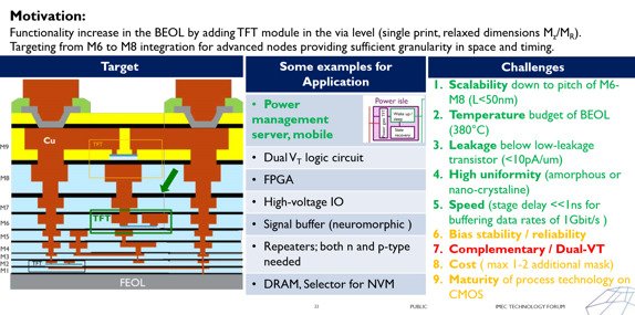
Toke also proposed that placing thin-film transistors in the interconnect might help with power management and be a potential solution in some applications.
Having observed the interconnect space for multiple years, I would expect Ru to emerge as the first measure to reduce the interconnect resistance, potentially followed or combined with another one of the solutions. However, the interconnect space is ripe with opportunities for breakthroughs to help drive the industry to 3nm.
3D May Save the Day
At the end of the day, (figuratively and literally) the industry is facing multiple challenges: Transistor scaling, interconnect scaling, and system scaling. One of the converging themes in all presentations was that 3D provides relief for multiple challenges.
Transistors and capacitors will continue to move into the vertical dimension as the industry drives to 3nm and beyond. Interconnect will continue to move vertically, but resistance-capacitance is a more formidable challenge that needs to be resolved.
Packaging is the area that seems to have the potential to not only continue the growth in the vertical dimension, but it also can remedy many of the challenges that are starting to limit the effectiveness of SoC. Developing a successful TSV silicon-to-silicon solution over the next few years may open the door to create the systems that will have the ability to create the AI systems that are being proposed today.


