

IFTLE has been saying for a few years that the decades-long scenario of moving from one node to the next was, for most if not all, dead and, that we had to keep our eyes open for what the next IC technology would be, because as we all know packaging only exists to protect and assist chips function.
Based on the 2019 Samsung Foundry Forum, which took place this May in Santa Clara, we certainly need to keep a close eye on Samsung’s new gates all around (GAA) technology.
Samsung announced plans to launch 7nm, 6nm, 5nm and 4nm process nodes in the coming years, with development tracks planned for 3nm. Samsung’s 5nm chips are expected in 2020, though prototypes can be made now. Samsung announced that its product design kit (PDK) for 3nm chips is now in alpha testing. The 3nm technology node will supposedly use this new GAA technology. Reports say it will speed performance 35% while cutting power use 50%.
IBM and its research alliance partners, Samsung and GlobalFoundries, first described the process they developed for making 5nm GAA transistors based on stacked nanosheets at the 2017 Symposia on VLSI Technology and Circuits conference in Kyoto, Japan. Other chipmakers, including Intel and TSMC, are known to be developing similar versions of next-generation transistors beyond FinFET similar to GAA FETs.
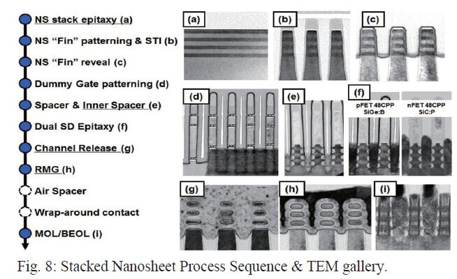
IBM/GF/Samsung’s reported process flow is shown in Figure 1.
A 300mm wafer of 5nm chips using GAA is shown in Figure 2.

GAA technology has been under development since the early 2000s by Samsung and other firms. GAA transistors are field-effect transistors (FET) that feature a gate on all four sides of the channel to overcome the physical scaling and performance limitations of FinFETs, including supply voltage.
TSMC, Samsung, and GF all announced FinFET designs for their 16nm and 14nm process nodes. The announced 14nm, 10nm, and 7nm nodes all FinFETs as well. Samsung has begun volume production on its 7nm FinFET process, the first to make use of next-generation extreme ultraviolet (EUV) lithography. Samsung considers 3nm to be its next major process technology node and the first that will use GAA, also called 3D multibridge-channel FETs.
There are two ways to build this new, gate-all-around (GAA) structure — nanowires and nanosheets. Nanowires are reportedly difficult to build but optimal for low-power. Nanosheets are believed to have advantages as far as performance and scaling are concerned, and Samsung the nanosheet approach for its 3nm node. It’s calling its GAA technology multi-bridge channel field effect transistor (MBCFET) (Figure 4).


The transistor gates control whether current flows across the channel. In the planar FET structure, the gate is on top of the channel. The newer fin FET designs raise the channel into fins with the gate built across it. GAA further encapsulates the channel completely with the gate. These structures are shown in Figure 4.

Compared to 7nm technology, Samsung’s 3GAE process is designed to provide up to a 45% reduction in the chip area with 50% lower power consumption or 35% higher performance.
Compared to FinFETs, the new architecture consumes far less power. Test results indicate a 40% boost in performance (at the same power as 7nm FinFETs) or up to a 75% savings in power compared with today’s advanced 10nm transistors.
The first 3nm chips currently aimed for smartphones and other mobile devices will be tested in 2020, with volume manufacturing expected in 2021. Introduction into graphics processors and AI chips packed into data centers are expected to arrive in 2022.
Handel Jones, of IBS, has stated that “Samsung is ahead of TSMC in GAA by probably 12 months ……and Intel is probably two to three years behind Samsung
For all the latest in Advanced packaging stay linked to IFTLE………………………………..


