
As this year’s 3D IC Test Workshop unfolded (September 12 & 13, 2012), one thing became increasingly clear to me: the challenge of probing microbumps is an item of critical concern in 3D test.
During the panel discussion on test requirements for 3D ICs, Saman Adham of TSMC Canada, noted that currently, microbump probing is extremely difficult and we need a better way to probe. Qualcomm’s Amer Cassier added that the reason for the challenge is the number of bumps needing to be probed, and poor signal integrity due to weak drivers. A stronger signal is needed to accurately test the interconnect capabilities of the microbumps.
The plot thickened during the Friday panel, How Will 3D Testing Change the 3D Supply Chain?, when Global Foundries, TM Mak, explained that with 2.5D and 3D IC technologies, cost/yield is paramount for 3D IC to survive and prosper, and that the level of known good die (KGD) “goodness” needs to increase. “97% is not good. 99% may not even be good enough when hundreds of dollars worth of good silicon is thrown away if you have a single bad die or even bad via.” he noted. “How do you get close-to-perfect silicon with lousy sort capabilities?”
Mak identified missing technologies and business processes affecting the 3D IC supply chain, among them probe test, test IP for non-contact I/O test methodologies, limitations of power-constrained sort, and yield ownership. Specific to probe test, Mak expanded on Cassier’s explanation of signal integrity and weak drivers, explaining that although there is some progress reported in tight-pitch probing technologies, the wide bus and the I/O are not designed for driving current to automated test equipment (ATE). Additionally, custom active probe cards and load boards are too expensive.
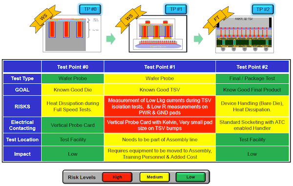
Amkor’s Gerard John explained his company’s approach to the 3D IC test flow. He identified three test points in the assembly flow, and assessed the risk levels of each. He explained that Test Point 0 uses a standard wafer probe to assess KGD, and carries low and medium level risk. The same is true for Test Point 2 – final package test. The issues clearly reside with Test Point 1, which tests for known good TSVs. Gerard identified these areas as medium to high risk, particularly with regard to low leakage and low R current measurements, and with vertical probe cards using Kelvin probes to touch down on very small pads on TSV bumps.
Questions Answered
To gain a better overall understanding of the problems and the potential answers, I turned to Imec’s Erik-Jan Marinissen for some explanations. He started with the basics:
TSVs form the interconnect from the front side of the die to the backside. Microbumps on the TSV pads form the interconnect between the two die. Today’s bumps are 40-50µm, and the technology exists to test them. However, explained Marinissen, 10µm diameter TSVs can be made, so the bottleneck in density lies with the microbump, therefore there is pressure to reduce the microbump size. He also stressed the importance of pre-bond testing before stacking to ensure yield.
Testing the C4 bumps on the bottom die is easy because they can be accessed from the bottom. The challenge comes in testing the microbumps on the top die. Pitches are too small for today’s technology. As noted previously in this post, manufacturers like TSMC and GlobalFoundries say they can’t probe microbumps below 50µm.
On the upside, there are lots of projects in the works to address these issues. Both Formfactor and Cascade Microtech presented papers on their probe technologies at the workshop, and earlier in the week at the International Test Conference, TSMC presented the probe test approach they take for their Chip on Wafer on Substrate (CoWoS) process flow.
TSMCs approach is targeted to testing its passive interposer used in CoWoS. The interposer is the lowest cost component of CoWoS, and stack yield depends upon interposer yield. Since it is not possible to test for KGD on the passive interposer because it only contains microbumps, TSVs, optical interconnects and C4 bumps, TSMC has come up with a “pretty good die” (PGD) solution that relies on optical interconnect probing from the front side through sacrificial pads, and TSV testing through C4 probing on the backside.

But according to Marinissen, this is insufficient. “Probing on test pads doesn’t really accomplish what you need because you can’t tell if the microbumps work,” he explained. “You’re adding a capacitive load for no good reason, which requires extra design time and extra space.”
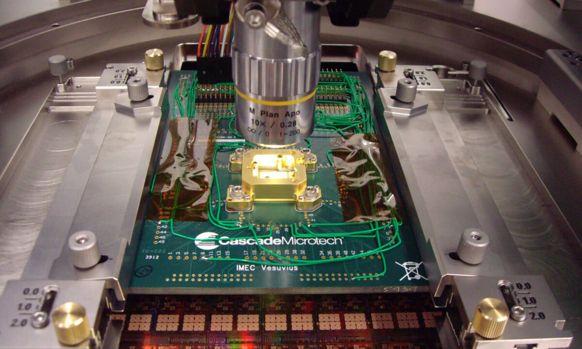
For some time, imec has partnered with with Cascade Microtech to develop tools and processes that would allow for probing directly on the microbump to initiate pre-bond test. The goal was to make good electrical contact with minimal damage to the microbump so as to affect the interconnect. In July, they reported success in probing 25µm diameter bumps using Cascade Microtech’s 300mm probe station and an advanced version of its Pyramid Probe technology. However, this is just the first step in a multi-step process before it can be used in volume manufacturing.
Formfactor, also a manufacturer of wafer probe technologies, has embarked on a similar mission with memory manufacturer, Elpida, with its Nanopierce contactor.
Marinissen clarified the primary differences for me. Both Formfactor and Cascade Microtech have probed the 40-50µm-pitch microbumps of the JEDEC Wide-IO DRAM interface. While FormFactor has demonstrated touching the four Wide-IO channels (4×300 bumps), the approach is limited to singulated die in a socket. Cascade and imec have only touched down on a single Wide I/O channel (300 bumps), but using a probe card solution, stepping over an entire 300mm wafer with a probe station.
In his presentation, Very Low Damage Direct Testing of Micro-Bumps for 3D IC Integration, Formfactor’s Onnik Yaglioglu explained that the Nanopierce contactor was developed to probe microbumps and micropillars for KGD and known good stacks (KGS). He reported that they have demonstrated full area contact and simultaneous probing of microbumps at 40-50µm pitch. Yaglioglu explained that the technology is highly scalable to achieve very dense pitch. Further, test set-up allows for precision alignment of the die under test to the contactor.
In his presentation, Signal Integrity Design for Wide I/O and 3D TSV IC Test at Wafer Probe, Cascade Microtech’s Ken Smith addressed that greater challenge described previously by Adham and Cassier. He detailed work being done on the signal integrity issue, identifying three elements to address including signal routing density, clean power delivery, and weak I/O driver limitations and progress in each area. He especially highlighted a breakthrough with the weak driver issue that involves pre-charging the tester interconnect to a large percentage of the predicted output level. This gives the weak driver the necessary boost to reach the right voltage level so that the microbump’s interconnect capability can be accurately tested by ATE. This is still in early stages so we can expect to hear more about this as the work unfolds.
These are just a few examples of the work presented at this year’s 3D IC Test Workshop. Proceeding of this event will be made available in the near future. ~ F.v.T.


A small remark about the terms “pre-bond testing” vs. “Known-Good Die (KGD) testing”. For me, the generic term for testing before stacking is “pre-bond testing”, as this term just refers to when in the production flow the test is carried out but carries no notion of the required test quality. “KGD testing” is a specific form of pre-bond testing, in which the test quality is as high as possible, as if this was a final test on a packaged device. KGD testing not only comprises high test coverage, but also coverage of at-speed defects and burn-in; items which are not always easy to realize at wafer probe.
Most test and product engineers will probably agree with me that some form of pre-bond testing is necessary to filter out most of the bad dies before they take other stacked good dies down under with them. Only in case of very high die yields, one can afford to avoid pre-bond testing. However, not necessarily do all these pre-bond test need to be KGD tests. Test application costs do not scale linearly with test quality; to get the last ppm’s (parts-per-million) of failing devices filtered out, you need a disproportional investment in test equipment and test time (especially if you want to run at-speed tests and burn-in during wafer sort). Hence, for many practical test flow scenarios, it will turn out more economical to do a first gross filtering in a pre-bond test which does not meet the quality standards of a KGD test (but is more a “Pretty Good Die” test, as some call it) and achieve the (ppm) defect level required by the customer during final (packaged) testing. What counts for the customer is that he/she gets functional parts with sufficient quality level for a reasonable price, independent of when and how that quality level was achieved. The trade-offs between pre-bond, mid-bond (on a partial stack), post-bond (on a completed stack), and final testing (on a packaged device) are internal to the die and stack makers’ operation.
Erik Jan Marinissen
EJ – Thank you once again for offering your input and perspective. I have a question regarding cost of test. At yesterday’s MEPTEC Semiconductor Roadmap Symposium, a couple of comments were made concerning cost of probe. One was that conventional probe technology doesn’t work for 3D IC test (that much we know) and that MEMS probers are too costly for standard products. Test schemes can’t overwhelm profitability. From the OSATS perspective, Ron Huemoeller of Amkor told me that while test will be critical for proving out a product, the likelihood is that at HVM, the practice will be to not test and take the final package yield hit. Any thoughts on this?
Hi Francoise,
In a 3D setting, with many natural/possible test moments in the overall stack manufacturing flow, “test” has two distinct objectives:
1. Making sure that the final stack product meets the quality expectations of the customer. The expected product quality (usually referred to as “defect level” or “test escape rate” and typically measured in Defective Parts Per Million (DPPM)) is obviously different in high-performance network infrastructure, handheld mobile consumer gadgets, and automotive applications (just to name three different markets).
2. Trying to avoid unnecessary cost downstream by weeding out bad components upstream. Here, test does have the role of, at the expense of some upfront investment, saving much higher cost later on, caused by the fact that one bad component renders its entire stack bad.
For the first goal, it does not matter where in the test flow the bad components are filtered out, as long as they get filtered out. Even if you do all your testing in the final test on the packaged device, for final product quality that would be fine. However saving all your test effort until the final product is ready, might not always be the best strategy economically speaking. For conventional 2D chips, it is very common to perform wafer testing, if only because it pays off not having to package dies which are identified as bad during wafer probe. You could perform a very high-quality wafer probe test (a so-called “Known-Good Die (KGD) test” to make sure no bad die gets packaged, but even a mediocre-quality wafer test can already save you a lot of otherwise wasted packages and packaging effort.
In 3D, this effect is amplified, as the die stack has much more value. That is why many companies are looking into pre-bond testing (testing before stacking) and mid-bond (on partial stacks) and post-bond (on complete stacks) testing. Performing these tests always comes with a price tag, but that might well lead to a downstream cost saving. A 10ct interposer die can kill a $100 SOC stacked on top of it. And hence, the cost of testing the interposer die should not (only) be evaluated in the light of the interposer value, but relative to the total stack value.
There is no “one-size-fits-all” 3D test flow. Its optimization depends on many factors, including yield and cost of components and process, and might even change over time as the production process matures. That is why at IMEC we have worked on a Test Flow Cost Modeling tool, together with TU Delft. The tool is called 3D-COSTAR and will be featured in a paper at next week’s IEEE 3D-IC Conference in San Francisco.
Coming back to your question. At last year’s 3D-ASIP Conference, I presented work that showed that (1) pre-bond testing pays off, and (2) expensive probe cards that are necessary to allow for direct probing of large-array fine-pitch micro-bumps are giving lower overall cost than the alternative, providing dedicated pre-bond probe pads. But that was for a particular set of parameters, yields, etc. So, the answer is: it depends. Ron might very well be correct for his products; but there are other cases as well.
Erik Jan Marinissen
Erik Jan,
Thanks for this comprehensive response. I look forward to hearing the paper next week at the 3D IC Conference. At the risk of oversimplification, I guess you could say that test will be more important when the device under test is for a high end application with a larger profit margin than for a consumer mobile application with smaller margins.
After reading the exchange, I can’t help but to put in my 2 cents.
It is not a matter of highend application or consumer mobile application. Every test operation has a cost associated with it, and correspondingly, there is also a cost associated with it if we do not test. In the case of delaying test to the end (and end up throwing away material and all the preceeding processing costs), the cost is not just a single chip, but all the chips integrated within that package. Some of these chips you have to pay for whether the final module is yielded or not. So, cost analysis between test and no test can be analyzed and decision made accordingly.
There is also the issue of responsibility. When something failed to work after you put them together, which element is faulty? Who should pay for it? Many of these PGD or KGD are delivered as claimed and used as it is extremely difficult to do incoming inspection by OSAT or the customer. So, if it turns out that the module (end product) fails in test, is it because some of these PGD/KGD/KGS (foundries) suppliers do not do their job properly or OSAT misprocess them? How do we know which party is at fault and be responsible? Sometimes, it is more than the money involved with RMA. The problem have to be traced back to the source and the process be fixed so that we can have functioning and profitable products eventually. So, the ability to diagnose is very important. All the test data from subsequent test steps also provide clues as to when the various processes start to introduce failures. So, intermediate test steps (and their data) are all important. In 2.5D/3D, we cannot wait til the end to test.
TM
Interesting discussion here – both Erik & TM make valid points.
I would like to take one step back (i.e. prior to the introduction of 3D packaging) – companies have debated if they prefer to do
(i) Light wafer test (shown as TP#0) in my chart, and then do the bulk of tests during final test (TP#2), or
(ii) Heavy wafer test and either a light FT or rely on a system level test (SLT) to screen defects.
From a test perspective, wafer test offers the advantage of lower Mean Time Between Assists (MTBA) and therefore higher efficiency than singulated final test. However, as Erik pointed out the cost differential for probe cards that test at “full device speeds” versus “low speed test” is significant, which adds to the cost of test.
It is imperative for the product engineer to evaluate the device cost (Dc) as a function of (i) point of test (PoT) (ii) cost of test (CoT) (iii) scrap costs (Sc). Where Sc is directly proportional to the yield.
Dc = f(PoT,CoT,Sc);
Once this equation has been computed, appropriate “points of tests’ can be inserted into the product flow.
Going back to the slide “3D IC Test points and their risk assessments”, TP#1 positioned at the Middle End of Line (MEOL) not only validates the TSV reveal process performed by the OSAT, but also checks the TSV fab quality (created at the fab). Once a sufficient quantity of wafers have run through this check point and enough data collected that classify these processes as mature, at that juncture TP#1 may only be used on a sample basis &/ or as a lot “look ahead” setup validation step.
One final point that I would like to make that addresses the panel discussion title “How Will 3D Testing Change the 3D Supply Chain?” – is the important role of academia in the supply chain.
While academia usually is strapped for access to funds / expensive 3D equipment that industry has access to, they are rich in two valuable resources that industry lacks, namely “time & fresh talent”. With fresh talent – I refer to minds that have not been exposed to the “processes of the past” that govern their “future thinking”. Such fresh talent, that have the luxury of time, and will bring in new ideas/ processess into the supply chain, that industry can evaluate and later adopt.