

A little over a year ago, I wrote a Knowledge Portal entry about the cost of 3D ICs. Here I am again to tackle the issue of 2.5D and 3D cost reduction from a slightly different angle. This entry is based on what SavanSys presented at IMAPS Device Packaging 2016.
The previous Knowledge Portal entry spent time discussing cost drivers; a few specific numbers were provided, but overall, the details were fairly general. While this Knowledge Portal entry is on a similar topic, it is not a continuation of the previous one. In this article, not only 3D will be examined, but 2.5D technology as well. Designs reminiscent of actual products on the market are analyzed, cost drivers are examined on a more detailed level, and a few cost sensitivities are tested. The main goal of this analysis is to identify opportunities for cost and price improvement for both of these technologies.
Although two technologies are included in this analysis, they are not being compared to each other. This is an analysis of cost drivers for both technologies without being a direct comparison—two totally separate designs are examined.
Activity Based Cost Modeling
Before breaking down the cost of the two technologies, an overview of the type of cost modeling used is necessary. Activity based cost modeling was used to construct both cost models used in this analysis. With activity based cost modeling, a process flow is divided into a series of activities, and the total cost of each activity is calculated. The cost of each activity is determined by analyzing the following attributes: time required, amount of labor required, cost of material required (consumable and permanent), tooling cost, all capital costs, and yield loss associated with the activity.
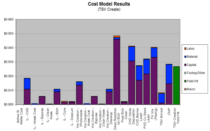
The graph below shows an example of the type of output that can be obtained from activity based cost modeling. These are the detailed steps for the through silicon via (TSV) creation process. The X-axis shows the name of the step; the Y-axis shows the type of cost that is contributing to each step.
Before leaving the topic of cost modeling, the concept of price versus cost should be addressed. The chart below shows a table of the cost components that make up price. While there are many components that go into price, only the direct cost is typically measured. The remaining cost components are applied as a percentage of direct cost. For mature technologies, competitive market forces drive the indirect and overhead costs to be predictable and consistent. A supplier with high relative overhead must either reduce their overhead or exit that market. As a market matures, only suppliers that can deliver products at a competitive price will survive. However, for new technologies such as 2.5D and 3D, the indirect and overhead costs can vary widely even though the direct costs will be similar across suppliers. For example, the equipment cost and throughput of deep reactive ion etch is approximately the same for everyone, but the overhead cost of a brand new factory may be very different than the cost of an established and partially depreciated factory.
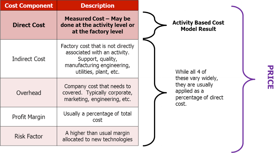
The goal of this analysis is to understand the direct cost drivers; therefore, all of the results are presented using relative costing. This removes all indirect costs, overhead, profit margin, and risk factor from the analysis.
Cost Breakdown
The cost analysis was performed on a design similar to the AMD Fury graphics product. This sample design includes four high bandwidth memory (HBM) stacks and a large GPU mounted on a silicon interposer. This design was chosen because it contains both 3D and 2.5D packaging technology. The 3D analysis is run on one memory stack consisting of one logic die on the bottom and four memory die on top. The 2.5D analysis includes the cost of the interposer, plus assembly of four HBM memory stacks and one large GPU.
Since both of these technologies contain many process steps, the following categories were chosen to summarize all results.
- TSV create – Includes all process steps required to create the TSVs in a normal thickness silicon wafer.
- TSV reveal – Includes all process steps required to thin the wafer and reveal the TSVs.
- Front-end-of-line (FEOL) – This is the RDL on the top of the wafer (interposer to die connection). Since fine pitch silicon die are mounted on top of the wafer, a damascene process is assumed.
- Back-end-of-line (BEOL) – Includes all activities performed on the bottom of the wafer (interposer to substrate connection). A WLP-style RDL and under bump metallization is assumed.
- Wafer bumping – Includes the cost of bumping either the active silicon wafer or the interposer in preparation for die bonding.
- Assembly – Includes all die bonding. Thermocompression bonding with NCP is assumed.
- Test – The cost to test all components with TSVs prior to assembly.
- TSV creation yield loss – The cost of scrap from TSV test failures.
- Assembly yield loss – The cost of scrap from die bonding failures.
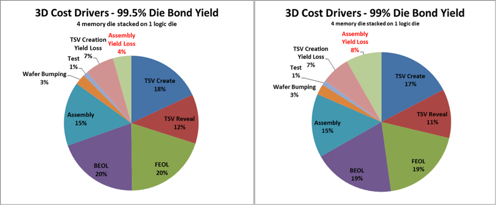
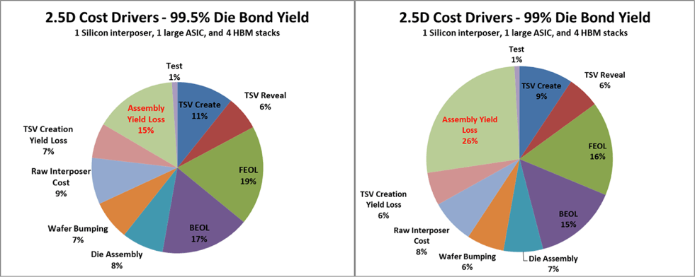
There are some key assumptions behind the following cost analyses. All die are assumed to be known good die (KGD), and the cost to fabricate the active die is not included in the analysis (except as part of scrap cost). The substrate fabrication and assembly are also not included in the analysis. High yields, at the level that would likely be needed for a mature process, are used. A 99.5% assembly yield is assumed for each die. In the 3D example, the thin wafer handling yield and TSV creation yield are assumed to be 98%. Those yields are both 95% in the 2.5D example, due to the fact that the 2.5D example deals with a larger surface area, and the same defect density in a larger surface area results in a lower yield.
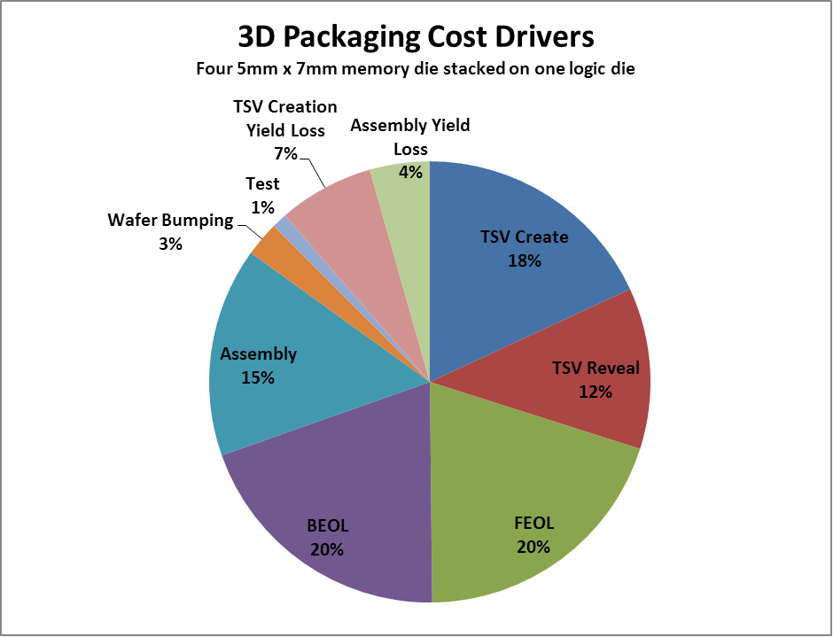
The pie chart above shows the cost breakdown by category for a 5mm x 7mm die stack consisting of five die. All costs associated with packaging are included, but the cost of the silicon die is not included. BEOL and FEOL costs are 20% each. The FEOL RDL is a more expensive damascene process than the BEOL RDL, but the BEOL also includes under bump metallization. Die assembly is 15% of the total cost since a relatively expensive thermocompression die bonding process is assumed.
The yield loss is divided into two categories because the amount of scrap is different between TSV fabrication yield loss and assembly yield loss. Once the TSV, FEOL, and BEOL processes are complete, the die can be tested before assembly. Bad die discovered during this test are scrapped before they are put on the die stack. However, defects introduced during assembly result in the scrapping of the entire stack. Although a high die bonding yield was assumed, the assembly yield loss is still significant because these defects are detected at the end of the process and result in everything being scrapped.

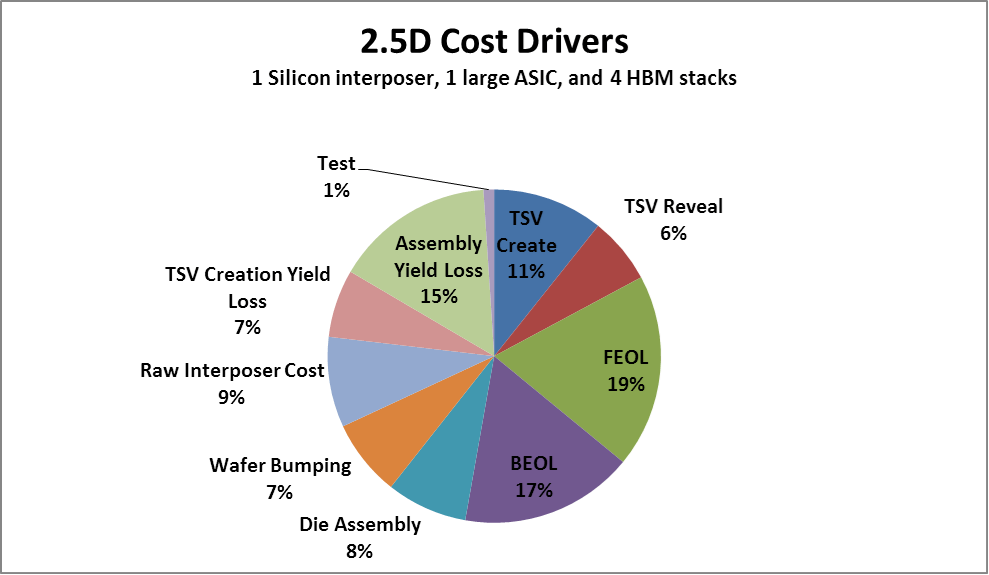
The pie chart above shows the cost breakdown by category of a 2.5D design consisting of a silicon interposer with four HBM stacks and one large ASIC. The TSV create and reveal activities account for about 17% of the total cost for this case, and the combination of BEOL and FEOL accounts for 36%. Most of this 36% is from the RDLs on both the top and bottom of the interposer. The raw interposer cost is significant given that the interposer must be large enough to accommodate four HBM stacks and one large ASIC.
TSV creation yield loss includes scrapping of the interposer but not scrapping of the ASIC or any of the HBM stacks. It is assumed that the interposer is fully tested before assembly. As with the 3D scenario, assembly yield loss carries a large cost because it will result in a complete scrap of everything. However, one of the tradeoffs that should be considered is increasing the test (currently 1% of the total cost) in order to reduce the assembly yield loss cost (currently 15%). One possibility is to assemble all the HBM memory stacks and then perform a test prior to assembling the ASIC since it is a much more expensive die than the memory stacks.
Sensitivity Analysis
Although the two technologies aren’t being directly compared, sensitivity analysis was carried out for the same variables for both technologies. This highlights some of the differences in cost drivers between the two processes.
The first variable looked at is the yield of the die bonding process. The same change—die bond yield dropping by half a percent—impacts the two technologies in different ways. The 3D assembly yield loss doubles, changing from 4% to 8% of the total cost. In the 2.5D case, this change results in assembly yield loss becoming one quarter of the total cost, instead of the already high 15%.
The other sensitivity analysis assumes that there were wafer probe defect escapes and resulting in failures at functional test. Total cost increase in the 3D case is 4.9%. For the 2.5D case, the total cost increase is only 1%, with the assumption that the HBM stacks are fully tested before assembly and contribute zero defects at final functional test.
Opportunities for Cost Improvement
Understanding where the cost comes from for each technology is not only useful for understanding where the technologies and process flows are currently, but for pinpointing potential areas for cost reduction. The following table identifies the areas in which impactful cost reductions may be made.
Conclusions
Many of the activities required for 2.5D and 3D packaging are already common activities done by a semiconductor fabricator. Activities such as imaging, CMP, damascene RDL process, wafer bumping, and a WLP RDL process will stay the same and make up a significant amount of the total 2.5D and 3D cost. However, other activities such as temporary wafer bond/debond, improved die and wafer assembly, and improved yields will cause the underlying direct cost of 2.5D and 3D packaging to improve. Improvements in overhead and margin driven by better factory utilization, more supplier competition, and improved process optimization specifically for 2.5D and 3D packaging technologies will have a significant impact on price.


are those assembly yield loss numbers used validated ? how do your total costs ( calculated by totaling various cost components ) for ea. HBM stack or the whole Fury – X module compare with numbers now in the public domain?
Thanks for your comment! Those assembly yields are the kinds of yields we would expect to see at HVM. So no, they are not necessarily reflective of yields today. As for your second question, the total costs are in line with what we have seen of Fury X prices in the marketplace.
Only 1% test costs for a complex multi-die chip like AMD’s Fury (consisting of an interposer base die with on top four four-die HBM stacks and a large GPU die) seems rather unrealistic to me. The DfT features aboard the GPU are likely to take >5% silicon area. Also the HBM DRAM stacks have built-in DfT features. These DfT costs should, in absence of a separate “DfT costs” category be attributed to “Test” costs. Also the total actual test execution costs of this complex stacked-die product are bound to be significantly larger than 1%; see the talks by AMD, SK hynix (the HBM DRAM supplier) and their suppliers FormFactor and Teradyne at the IEEE 3D-TEST 2015 Workshop (http://3dtest.tttc-events.org).
We definitely agree that there is a significant amount of testing required for a design as complex as the AMD Fury. We also believe the testing cost is quite high today and will decrease over time. However, for this analysis we did not include any testing other than basic open short testing to find defects created during assembly. Our pie charts do not include wafer probe test, functional test, or burn in test. That is why our estimated test time is so small compared to the total test time to build and manufacture the complete product. That being said, we also believe that even the open short testing today is higher than our estimate, but will improve significantly as the product moves into HVM.