
 We are pleased to announce the winners of the 2018 3D InCites Awards, sponsored by KLA-Tencor and EV Group and hosted by iMAPS. This may have been the most exciting awards year yet, with 40 nominees from 26 companies and four research institutes competing for awards in 9 categories. The competition was fierce! We logged in over 40,619 online votes, more than twice the number of last years event. The category with the most votes was Equipment Supplier of the year, with 9581 total votes. The next highest was Process of the Year with 6184 votes
This year’s awards will be presented during the iMAPS Device Packaging Conference, March 7, 2018, in Fountain Hills, Arizona. All nominees, winners, and attendees of IMAPS DPC are invited to attend the 3D InCites Awards Ceremony and Barbecue, to benefit the iMAPS Foundation and Phoenix Children’s Hospital. Based on the theme, “Building a Brighter Future Through Health and Education”, be prepared for a fun-filled evening with games and prizes and the opportunity to donate to some great causes.
Congratulations to this year’s winners! We look forward to celebrating with you!
Device Manufacturer of the Year: Amkor Technology
The company was nominated for its acquisition of NANIUM, now Amkor Technology Portugal (ATEP). The company is now a leader in 300 mm wafer-level packaging, including both fan-in wafer level chip scale packaging (WLCSP) and WLP, both fan-in wafer-level chip-scale package (WLCSP) and wafer level fan-out (WLFO), based on embedded wafer level ball grid array (eWLB) technology.
Device of the Year: M-Series ™ Deca Technologies, and OS05A20 Image Sensor with Nyxel ™ Technology, OmniVision Technologies
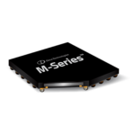 Deca Technologies’ M-Series was nominated for addressing some of the key limitations the incumbent approaches faced courtesy of the adaptive processing combined with planar front side molding. The investment of over $110m in Deca by two of the giants of the industry is a testimony to this technology. In particular, M-Series is the only WLFO solution with Adaptive Patterning™, which accommodates die shift, thereby resolving yield issues that may occur due to the placement tolerance.
![]() OmniVision’s OS05A20 Image Sensor was nominated for being the first of its image sensors to be built with Nyxel ™ Technology. This approach to near-infrared (NIR) imaging combines thick-silicon pixel architectures with careful management of wafer surface texture to improve quantum efficiency (QE), and extended deep trench isolation to help retain modulation transfer function without affecting the sensor’s dark current. As a result, this image sensor sees better and farther under low- and no-light conditions than previous generations.
OmniVision’s OS05A20 Image Sensor was nominated for being the first of its image sensors to be built with Nyxel ™ Technology. This approach to near-infrared (NIR) imaging combines thick-silicon pixel architectures with careful management of wafer surface texture to improve quantum efficiency (QE), and extended deep trench isolation to help retain modulation transfer function without affecting the sensor’s dark current. As a result, this image sensor sees better and farther under low- and no-light conditions than previous generations.
![]() EDA Supplier of the Year: Mentor, A Siemens Business
EDA Supplier of the Year: Mentor, A Siemens Business
Mentor was nominated in recognition of the efforts of Juan Rey, VP of Engineering, at a number of 3D-IC focused conferences in 2017. Rey conveyed not only Mentor’s capabilities in supporting 2.5/3D-ICs, but also explained why and where EDA tools and designX methodologies are important for developing cost-effective solutions and get them right the first time.
 Engineer of the Year: Gill Fountain, Xperi
Known as Xperi’s guru on Ziptronix’ technologies, Gill was nominated for his most recent contribution, expanding the chemical mechanical polishing process window for Cu damascene from relatively fine features. His team developed a process that delivers uniform, smooth Cu/Ta/Oxide surfaces with a controlled Cu recess with very small variance across wafer sizes. He has been an integral part of Xperi’s technical team and his work allows the electronics industry to apply direct bond interconnect (DBI) for high-volume die-to-wafer applications.

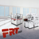 Equipment Supplier of the Year: FRT GmbH
FRT was nominated to recognize FRT MicroProf®, its third generation of surface metrology tools that combine multi-sensor technology and hybrid metrology in one measuring system. The MicroProf® uses optical multi-sensor technology to measures the topography and the total thickness or the film thickness of your samples without contact. It can carry out a wide range of measurement tasks for 3D IC, Advanced Packaging, and MEMS applications quickly, efficiently and intuitively.
![]() Material Supplier of the Year: Semblant
Material Supplier of the Year: Semblant
Over the past 12 months, Semblant has seen a rapid and widespread adoption of its MobileShield technology, a repeatable, sustainable, cost-effective nanocoating solution that protects mobile phones from water damage and corrosion, the leading causes of mobile device failure. Consumers spent $23 billion repairing devices in 2017 alone. Semblant is working with 9 of the top 11 smartphone manufacturers in the world to protect the world’s latest flagship mobile devices, having achieved Ingress Protection (IPX) 7 certification for MobileShield in 2017. The company has also opened a dedicated Customer Innovation Center in Shenzhen, China.
 Process of the Year: F.A.S.T., KOBUS
F.A.S.T. was nominated for combining the best of CVD and ALD deposition worlds: high deposition rate, high conformity, process flexibility, low process temperature performance & tool simplicity. Already demonstrating its uniqueness for TSV application, the F.A.S.T. deposition solution is becoming the reference when thick and conformal films are needed in applications such as advanced interconnects, photonics on IC, MEMS, 3D LED, µ-displays and much more.
 Research Institute of the Year: Fraunhofer IZM
Fraunhofer IZM was nominated for launching a consortium to bring research and industry together on all questions of implementing panel level packaging (PLP) in industry settings. Their aim was to accelerate standardization, develop a low-cost, industry-ready reference process and channel ongoing research advances into the industry as quickly and efficiently as possible. Progress to date has been good, and the Fraunhofer IZM activity in the PLP space has received much notice.
 Startup of the Year: KOBUS
KOBUS was nominated for developing a unique deposition solution to leverage the integration cost issue of TSV. With thick and conformal capabilities, the tool and process solution offers unique film properties at a low temperature allowing for a drastic reduction in film thickness requirements, and thus can be extended to very high density and high aspect ratio features (> 20:1). There is a 25% reduction of integration cost, thereby dividing by two, the total Cu removal thickness before CMP. One tool answers both via middle and via last TSV integration requirements. Relaxed via opening etch step results in conformal engineering along the TSV shape.
Thank you to all the nominees and everyone who participated! We look forward to celebrating with the winners next week.


Comments are closed.