Latest Posts - Page 13

Stay Virtually Connected with Your Industry Colleagues and Favorite Topics at ECTC 2020
On behalf of the entire Program and Executive Committees, it is my pleasure to invite and welcome all of you...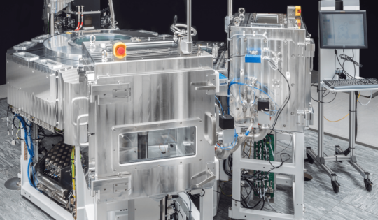
SPTS Technologies Honored with Queen’s Award for Enterprise in Innovation 2020 for its Mosaic™ fxP Plasma Dicing System
Prestigious Award Recognizes SPTS’s Plasma Dicing Innovation in Advanced Packaging Technologies for the Global Semiconductor Industry NEWPORT, UNITED KINGDOM, 21...
IFTLE 450: Chiplet is the New Buzzword but Disintegration is the New Technology
Funny how language works and how new terms enter our lexicon. IFTLE is not a supporter of buzzwords. As a...
IMAPS Announces a Suite of Virtual Learning Opportunities for the Semiconductor Packaging Industry
A live webinar on Recovery and Growth Areas After COVID-19 kicks off virtual programming May 20th. [May 15, 2020 –...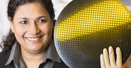
IFTLE 449: Advanced Packaging and Chiplets at the IMAPS DPC
ECTC Meeting Goes Virtual For those that have not seen the announcement, the Electronics Component Technology Conference (ECTC) held annually...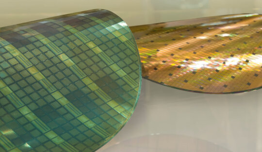
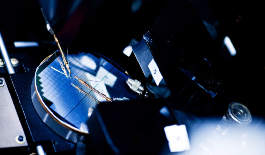
Temporary Wafer Bonding System Is Based On Electrostatics, Not Adhesives
Temporary wafer bonding is widely employed in semiconductor device fabrication and in semiconductor device packaging applications, particularly now that changes...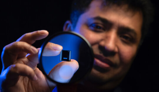
Chiplets: The New Era Begins
The semiconductor industry has entered a new era and the role of design including the package has become increasingly important....
5G, AI, and Server Markets Provide Growth, Despite Pandemic
Despite the economic downturn caused by the fight against the Covid-19 virus pandemic, there are some potential growth areas this...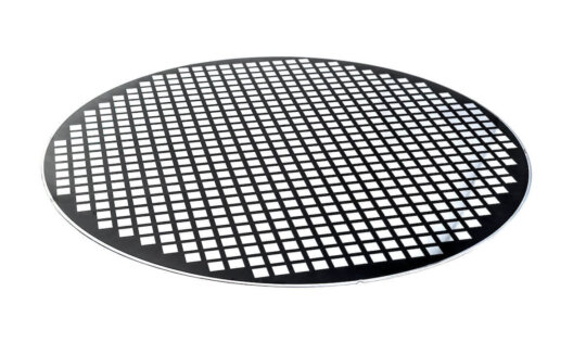
Temporary Bonding and Mold Process to Enable Next-Gen FOWLP
Temporary wafer bonding processes were initially developed for enabling three-dimensional (3D) stacked integrated circuits (ICs). For example, dies can be...

IFTLE 448: Impact of Package Pitch on PCB Fabrication
While the focus of IFTLE remains on the latest advances in advanced chip packaging, we have mentioned before that we...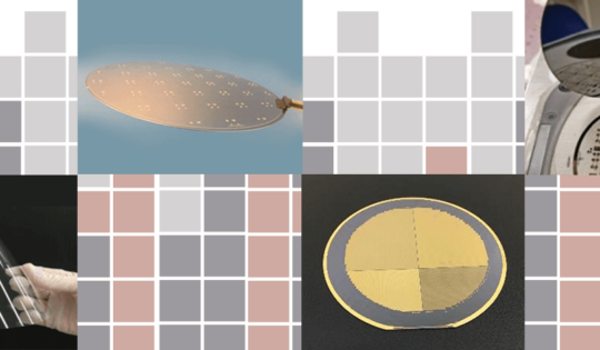
Mosaic Microsystems Wins Two SBIR Awards to Support Technology Development Initiatives
Mosaic Microsystems, a microelectronics and photonics packaging company providing thin glass substrates and through glass vias (TGVs) for next generation...
IFTLE 446: 2.5/3D Inspection; Embedded Chip Tech; Wide Bandgap Semi Roadmap
Let’s look at a few more presentations from the SEMI 3D & Systems Summit which was held in late January...Mosaic Microsystems Secures $2 Million Seed Round from BlueSky Capital and Corning
Rochester, NY — Mosaic Microsystems, a microelectronics and photonics packaging company, providing thin glass substrates and through glass vias (TGVs) for...
Smoltek patent No. 57 now granted
Smoltek keep growing its proprietary technology platform. In March 2020, the 57th patent was granted. This is a Pan-European patent...
ACM Research Launches Stress-Free Polishing Tool for Advanced Packaging Applications; Delivers First Tool to Leading Chinese OSAT
Ultra SFP ap Provides Environmentally Friendlier Alternative to Conventional CMP for TSV and Fan-Out Wafer-Level Packaging Processes Fremont, California –...
Coronavirus Gives Rubbing Elbows a New Meaning at IMAPS DPC 2020
As the domino effect of electronics industry event cancellations continued in response to the global threat of a potential Coronavirus...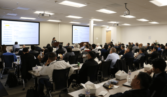
Has Google Discovered the Advantages of Advanced IC Packaging Technologies?
At the latest MEPTEC Luncheon, held February 5, 2020, and hosted by SEMI at its Milpitas HQ, Google’s Dr. Preeti...
Emerging Market for Low-Density Panel FO Analyzed
Large area fan-out (FO) remains a hot topic in the industry. There is some confusion over the term “panel” because...