
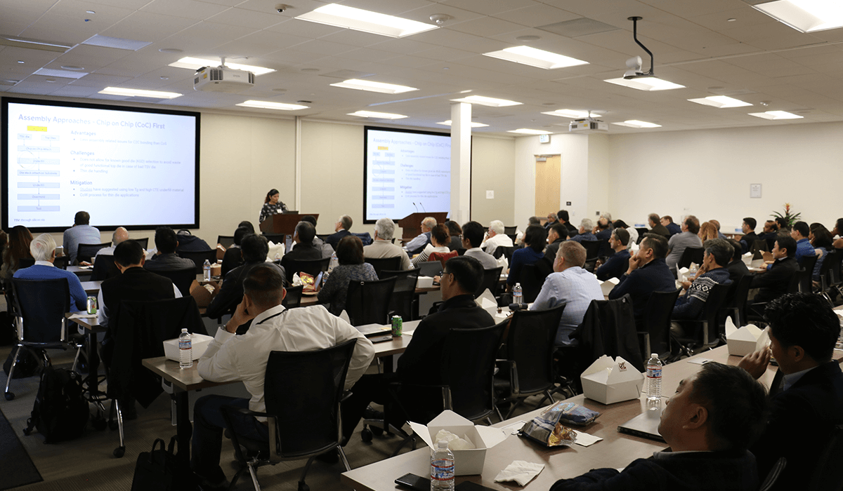
 At the latest MEPTEC Luncheon, held February 5, 2020, and hosted by SEMI at its Milpitas HQ, Google’s Dr. Preeti S. Chauhan, Technical Program Manager for Data Center Quality, presented her perspectives on the benefits and challenges of advanced IC packaging technologies.
Considering that Alphabet, Google’s parent company, controls about 400 companies directly or indirectly, I noticed that the almost 200 attendees followed her message very attentively. Alphabet’s subsidiaries, like Waymo (Automotive), Fiber (Internet), Calico (Life Sciences), Nest (Smart Homes) as well as hardware for Google’s Data Centers supporting Android (Smartphones), YouTube (Video), Maps (Guidance), Google Ads and other services, offer lots of opportunities for advanced IC packaging technologies.
The worldwide market opportunity
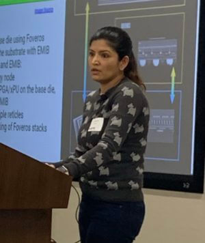
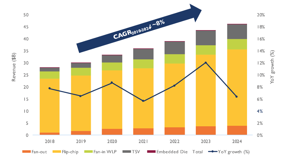
Chauhan confirmed that packing lots of functionality into single-die ICs is reaching technical and cost limits. Interposer-based multi-die ICs (a.k.a. 2.5D-ICs), comprised of chiplets, represents a very good solution for improving performance per Watt in data centers. She substantiated the revenue opportunities for advanced IC packages with this slide from Yole Developpement, (Figure 2) and also showed two slides from Goldman Sachs about the hardware needed for AI computing.
The first slide from Goldman Sachs showed the Total Available Market (TAM) for AI compute-hardware growing from about $ 10 Billion in 2019 to almost $ 60 B in 2025, representing a 40% Compound Annual Growth Rate (CAGR). The second slide split the projected AI computing TAM in 2025 into the functions likely to be needed and estimated their respective revenues: CPUs 5.8 B, GPUs 31.2 B, ASICs 5.8 B, and FPGAs 12.2 B.
Major Suppliers Offer a Broad Range of Advanced Packaging Technologies
Chauhan gave an overview of advanced packaging solutions major players have developed. She explained Intel’s embedded interconnect bridge (EMIB) and Foveros technologies, as well as the combination of them, called CoEMIB. She outlined SPIL’s silicon-less interconnect technology (SLIT) and ASE’s fan-out chip-on-substrate (FOCoS) as well as TSMC’s integrated fan-out on substrate (InFO_oS) solution. Chauhan emphasized that warpage challenges need to be minimized and the “good old” known-good die (KGD) challenge needs to be addressed with innovative system and IC architectures as well as new design and test methodologies, before high-volume manufacturing of multi-die packages will become attractive widely, even for cost-sensitive applications. Riko Radojcic’s book More than Moore Technologies. explains these and other advanced packaging technologies and their building blocks in depth.
Observations with Multi-die IC
In general, heat management is the biggest challenge in data centers. Interposer-based (2.5D) designs make it easier to cool dice operating in high-performance applications. Chauhan noted that the manufacturing steps for TSVs are rather complex and costly and that micro-bumps can lead to voids in underfill materials and heat-flow disruptions. The currently relatively high reflow temperatures cause interposer and thinned die warpage. Coper-to-copper (low temperature) hybrid bonding requires very clean surfaces to benefit from the much tighter interconnect spacing it allows. Also, very high current densities in micro-bumps can lead to electromigration, resulting in contact failures.
Summary of the Q&A Portion and a Few Personal Comments
The large audience asked significantly more questions during this event than at any one of the previous MEPTEC Luncheons I have attended. Chauhan addressed all the in-depth technical questions very well but didn’t comment (for competitive reasons?) on a few of the business-related topics.
It’s great to see that successful companies are investing significantly in analyzing the strengths and (current) weaknesses of advanced IC packaging technologies. Based on her role at Google, Chauhan’s presentation covered these technologies from a data center perspective. I hope that we (the MEPTEC Luncheon organizers) will also be able to attract speakers from other large semiconductor customers. As outlined at the beginning of this blog, the Waymo Team would have a lot to say, e.g. about sensors, Fiber about electrical & optical interfaces, Calico about multi-die benefits and reliability requirements in very space and power-constrained medical applications and Nest about the broad range of consumer applications in a home or office. Likewise, other system houses, focused on networking, industrial, automotive, Mobile, Medical, etc. applications are very welcomed to present at future MEPTEC Luncheons.

Chauhan’s presentation about her work at Google was very informative and useful for supply chain engineering experts. If you are a packaging expert in one of the big system houses or know such a person, please help us educate the supply chain (MEPTEC stands for Microelectronic Packaging and Test Council) at one of the future luncheons. Educated suppliers can offer customers more suitable solutions, and sooner. Please contact either Ira Feldman at ira@feldmanengineering.com or me at herb@eda2asic.com, if you can talk about your microelectronics packaging and test requirements or can motivate another expert user to present his/her observations and requirements.
As Chauhan emphasized in her presentation, know good die (KGD) is a hot discussion topic and critical for the success of multi-die ICs. MEPTEC has organized a full day KGD workshop. Please join us at SEMI in Milpitas on Tuesday, April 21, to discuss with KGD experts and contribute ideas as well as your requirements for this topic.
Last, but not least, please join us at the next MEPTEC Luncheon, to be held at SEMI on March 11. Paul Pickering from MicroTech Ventures will talk about “Geopolitics and Manufacturing”. That’s a very relevant topic today, for everybody working in the semiconductor supply chain.
Thanks for reading……Herb
Disclaimer: The opinions presented by Dr. Preeti Chauhan are exclusively her own, based on her research, and don’t reflect the opinions of Google.


