

Funny how language works and how new terms enter our lexicon. IFTLE is not a supporter of buzzwords. As a matter-of-fact, we detest buzzwords about as much as we detest political correctness. We all heard the term nanotechnology used until it nearly made us gag. For me, ditto the use of the term “internet-of-things” which still has no real meaning for me, and of course there is “Moore’s Law” (which is really not a law, but rather an observation). Currently, the buzzword that all researchers are wanting to link themselves to and align themselves with is “chiplet”. I hate it when a term that one uses all the time turns into a buzzword.
As we outlined earlier this year in the 3D InCites Yearbook article “Disintegration is Underway,” the long-held contention that integration will forever lead us forward has been challenged in the last few years by those supporting what is, for all intents and purposes the antithesis – disintegration. Basically, the rising costs of smaller node technologies and ever-larger chip sizes have taken us to a point where one can envision smaller, less costly functional chiplets connected within a package by high-bandwidth connections, as a less costly solution.
Widespread adoption of chiplets, with roots in the multichip module technology of the 1990s and more recently the system-in-package (SiP), would certainly be a paradigm shift for our industry. My point here is that the technology is disintegration and the physical expression of that technology is the use of chiplets to fabricate our newest devices.
The latest to join the chiplet bandwagon is Digitimes who recently announced that “…. a new approach to semiconductor design and integration has arrived: the chiplet, which promises to help restore the microchip industry to its historic rate of advancement.” (Oh no… I think they are about to link chiplets to Moore’s Law!)
They continue “… in recent years… semiconductor production processes have encountered physical limitations at extremely small sizes. Chiplets …replace a single silicon die with multiple smaller dice that work together in a unified packaged solution. This approach provides much more silicon to add transistors compared to a monolithic microchip. As a result, chiplets are expected to allow a return to the two-year doubling cycle that has underpinned the economics of the semiconductor business since 1965.” Yes, the contention here is that chiplets will save Moore’s Law. In truth, you cannot “save” an observation. It is either right or wrong and Moore’s observation was certainly correct for a long period of time, but now it simply is not.
Digitimes then reports that market research company, Omdia, sees the MPU segment representing the largest single market for chiplets, with the global market for chiplet-enabled MPUs expected to reach $2.4B by 2024. As we know MPU suppliers Intel and especially AMD have been early innovators building proprietary advanced packaging chiplets. Further out, Omdia expects chiplet revenue to reach $57 B by 2035 much of the growth driven by “…chiplets that serve as heterogeneous processors, i.e., chips that combine different processing elements, such as applications processors that integrate graphics, security engines, artificial intelligence (AI) acceleration, low-power internet of things (IoT) controllers and more.”
ISSCC 2020
The recent IEEE International Solid-State Circuits Conference (ISSCC) included advanced packaging technology papers from CEA Leti, Intel, and AMD.
CEA Leti – 96 Core Processor with Six Chiplets 3D Stacked on an Active Interposer
Leti contends that “…in the context of high-performance computing and big-data applications, the quest for performance requires modular, scalable, energy-efficient, low-cost manycore systems.” Partitioning the system into multiple chiplets and connecting them with 2.5D interposers or silicon bridge structures leads to large modular architectures and cost reductions. [The cost reduction part is yet to be proven!]
The Leti presentation describes an active interposer integrating: (a) a switched capacitor voltage regulator (SCVR) for on-chip power management (voltage-regulation systems that are usually found on the processor itself); (b) flexible system interconnect topologies between all chiplets for scalable cache coherency support; (c) energy-efficient 3D-plugs for dense inter-layer communication and (d) a memory-IO controller and PHY for socket communication.
The chip (below) integrates 96 cores in six chiplets in 28nm FDSOI CMOS, 3D stacked in a face-to-face configuration using 20μm-pitch μ-bumps onto a 200 sq. mm active interposer with 40μm-pitch through silicon via (TSV) in a 65nm technology node.

Figure 1: Chip microphotographs, 3D cross-section, package, and technology features. (Courtesy of CEA-Leti.
The circuit is fully testable for known good die (KGD) sorting of both chiplets and the active interposer, and for final test, using compressed full scan, IJTAG for 2D IO and 3D IO boundary scan, BIST engines, and dedicated test pads.
Intel – A 3D Stacked 10nm & 22FFL Hybrid Processor in 12 sq mm

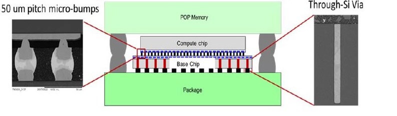
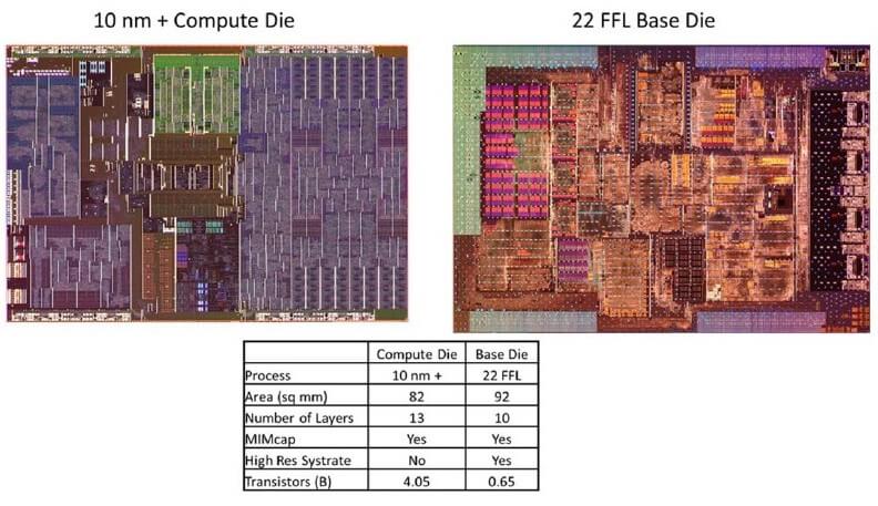
Intel used its 3D integration tech, Foveros, to produce the new Lakefield mobile processor. Foveros provides high-data-rate interconnects between chiplets by stacking them atop one another and delivering power and data from the package vertically through the bottom die. The stacked die and implementation of the 3D package with package-on-package (PoP) memory is shown in the figure below. The compute die is Intel 10nm+. The memory subsystem supports LPDDR4X PoP in a 4×16 configuration. The base die is Intel 22FFL and contains the chipset functionality including PCIe Gen3, USB type-C, storage, audio, and a sensor hub. Combining 10nm and 22FFL in 3D enables a large dynamic range of performance and power modes. The 3D dies communicate with a low-power inter-die I/O called the Foveros Die Interface (FDI).
The two dies are stacked vertically face-to-face with a dense array of 50μm pitch µbumps. The base die in 22FFL includes TSVs to route power and signals to the package. The LPDDR4 PoP memory is integrated using a through-mold via at a 350μm pitch. Lakefield supports two- or four-high stacked DRAM. Vertical integration of the chipset functionality and memory with a simplified PMIC power delivery allows Lakefield to fit in a 12mm×12mm x1mm (height) small form factor.
High micro-bump density is maintained over potential hotspots in the compute die to compensate for the reduced thermal spreading in a thin-die stack. The high array density of the power TSVs also reduces the C4 bump temperature.
AMD – Chiplet Architecture for High-Performance Server and Desktop Products
This was kind of a review paper for the ISSCC audience explaining why AMD chose to go with chiplet technology for their processors. We have covered most of this in previous chiplet blogs.
AMD described how they used chiplet technology for their second-generation EPYC high-performance processors “Rome” and “Matisse” to achieve performance/$ and performance/W, targets for server and client markets. Both the Rome and Matisse products leverage the same CPU chiplets. The chiplet architecture enabled them to use leading-edge 7nm CPUs for multiple markets with high reuse for improved time-to-market. It is well known that shrink factors in advanced nodes are much lower for analog circuitry than for digital logic and SRAM. By keeping the memory interfaces and SerDes in mature 12nm technology, costs are mitigated since those circuits see a very small shrink factor performance or power gain from advanced nodes. They report that the modularity of chiplets enables product configurations not achievable with monolithic designs. They stated that server/client top end core counts (64 and 16 resp.) would not be practical in a monolithically integrated chip, and in the case of the 64 core server part, way beyond maximum reticle size.
The previous generation had been made up of four chiplets. But in order to fit more silicon in while keeping costs down, the company redesigned the chiplets so that only the computing cores were upgraded to TSMC’s 7nm technology. All other functions were included in a chiplet made using older, less costly technology.
They conclude that “chiplet architecture required significant advances in engineering the package, interconnect, test and power management infrastructure, but enabled product configurations across multiple markets that are far more performant and cost-effective than otherwise possible”.
For all the latest in advanced packaging stay linked to IFTLE…………………….


