
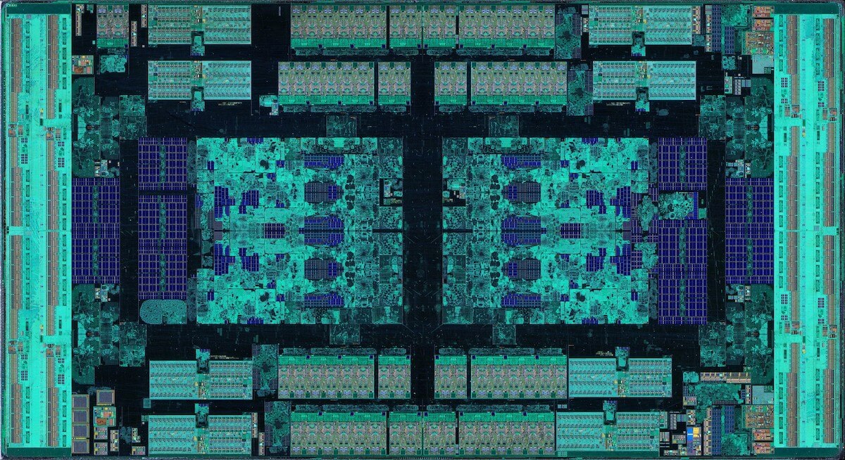
 In 2017, AMD used chiplets in their “Zen 2” architecture to develop the Epyc server processor “Naples” (Figure 1). AMD engineers estimated a system-on-chip (SoC) design would have more than doubled the manufacturing cost and significantly increased the development time.
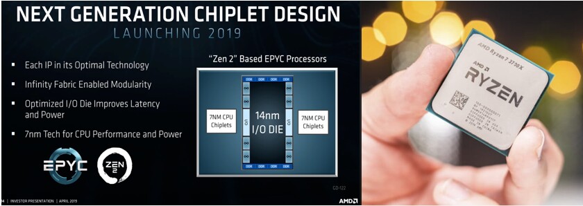
AMD is now deploying its “Zen 2” chiplet technology in Ryzen, 3rd generation consumer CPUs (Ryzen 3000s), as well as its next-generation enterprise EPYC processor, known as Rome.
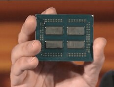
While the previous processors used up to four Zen CPU modules, the Ryzen 3000 includes multiple Zen 2 CPU modules (8 core chiplets) fabricated with TSMC 7nm technology as well as an I/O die made using a mature 14 nm process technology. This allows the I/O portion which is less sensitive to clock speeds and power to use the older 14nm process, while the CPU chiplets use 7nm to get peak performance (Figiure 2).
The IO die controls off-chip communications, housing PCIe lanes for the processor, memory channels, and links to other chiplets or other CPUs.
The consumer processors, Ryzen 3rd Gen or Ryzen 3000, will be offered with up to two chiplets for sixteen cores.
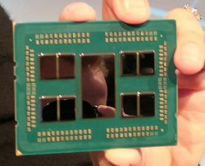
The IO die for the EPYC Rome processors uses GlobalFoundries’ 14nm process, however, the consumer processor IO dies (which are smaller and contain fewer features) are built on GlobalFoundries’ 12nm process. The EPYC Rome processors, built on these Zen 2 chiplets, will have up to eight of them, enabling a platform that can support up to 64 cores. As with the consumer processors, no chiplet can communicate directly with each other – each chiplet will only connect directly to the central IO die. That IO die houses links for eight memory channels and up to 128 lanes of PCIe 4.0 connectivity.
The I/O die will feature “Infinity Fabrics” (substrates) to connect chiplets and 8 DDR DRAM interfaces. The memory controller is now located inside the I/O die giving the CPU chiplets more equal memory access latency.
Separating CPU chiplets from the I/O die has its advantages because it enables AMD to make the CPU chiplets smaller, thus using less 7NM technology, theoretically making the module less expensive to manufacture.
The Need for Chiplet Standardization
To get widespread adoption of chiplet technology we must have standardization of the I/O interfaces; i.e a chiplet made by company A must be able to talk to a chiplet made by company B. The DARPA CHIPS program has focused on the Intel AIB protocol.
More recently TSMC, who as you learned above is fabricating chiplets for AMD, announced their lipincon protocol.
In Sept. the Chiplet Design Exchange (CDX), comprising zGlue, Ayar Labs, Avera Semi, ASE, Cadence, Netronome, and Sarcina, announced as part of the Open Compute Project(OCP), a subproject to standardize design automation for the impending chiplet marketplace. The group is tasked with standardizing machine-readable chiplet models to enable chiplet catalogs and provide reference flows for the development of chiplet-based modules.
The CDX group surveyed the industry to understand the needs and concerns for chiplet information exchange and published those results. The group is now working on a whitepaper with the proposed formats and recommendations to create a catalog of available chiplets and further demonstrate the proof-of-concept in a package (figure 2).
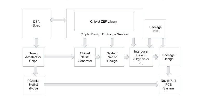
CDX plans to create a proof-of-concept based on PCIe while developing its PHY, protocol and other specs. The group also aims to define a business flow for chiplets and define a test certification for known-good chiplets. EE Times reports that the group “appears to have rejected Intel’s AIB protocol (which is being used at DARPA CHIPS) as being too limited in data rates and pinouts”.
Agreement on chiplet standardization must come if this is to become the next great wave of chip manufacturing.
For all the latest on advanced packaging stay linked to IFTLE……………….


