
Let’s look at a few more presentations from the SEMI 3D & Systems Summit which was held in late January in Dresden.
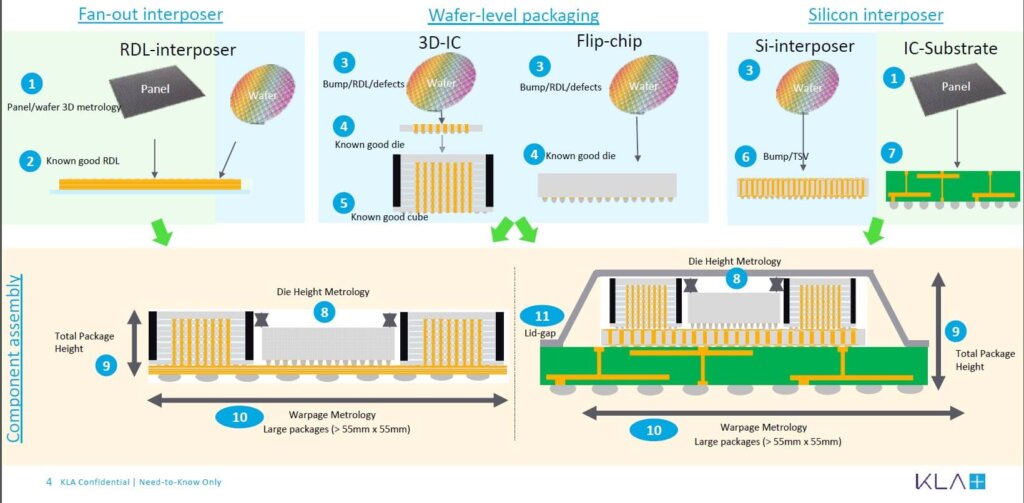
KLA showed this interesting schematic of where inspection was necessary for high-density 2.5/3D packaging.
Embedded Chip Technology
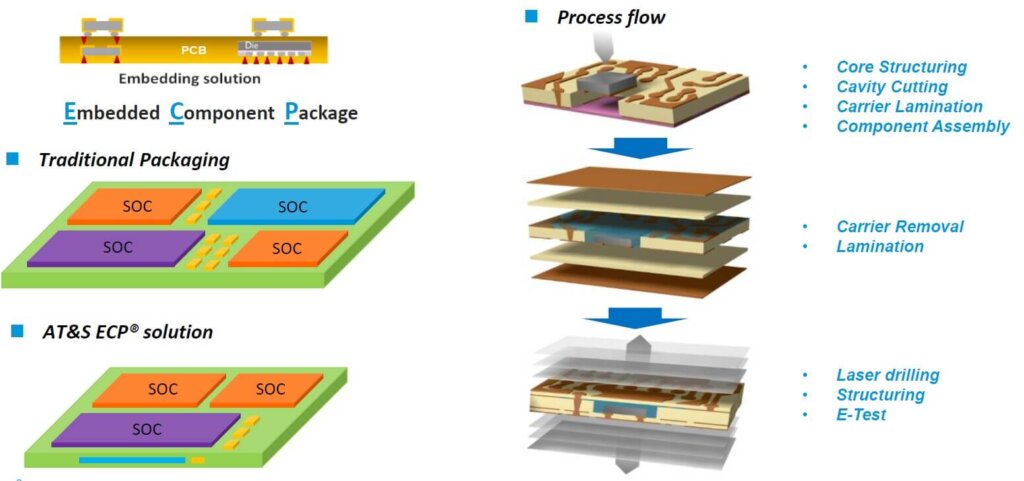
AT&S gave an interesting presentation on “Heterogeneous Module Integration using Embedded and Cavity Technologies on Advanced Substrates”. Embedded chip technology in advanced PCB substrates is a technology that has been around commercially for nearly a decade, but we have yet to see it really take off. That isn’t to say that it will never take off. Recall the history of fan-out packaging. Infineon was the only user of eWLB for many years till the technology finally caught on, especially when TSMC adopted a variation of it. Anyway, embedded chip technology is one of these technologies that really makes sense on PowerPoint slides, but has not caught the imagination of the packaging community…YET. Their proposal for what they call embedded component packaging is shown below.
Of course, such embedding technology can only be used on components where thermal requirements can be met while embedded.
Below is a slide that AT&S uses to explain the benefits of using their cavity technology.
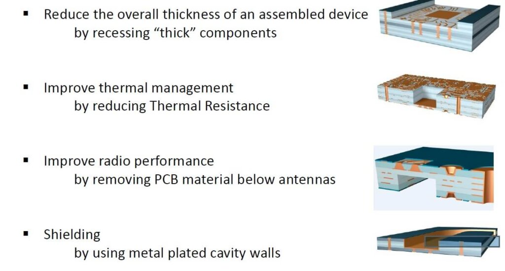
Thus, where applicable, embedded chip technology could certainly give you a smaller form factor and cavity technology could certainly offer performance advantages.
Roadmap for Wide Bandgap Power Semiconductors
Changing topics for a moment, the use of wide bandgap (WBG) semiconductors silicon carbide (SiC) and gallium nitride (GaN) in the power industry is receiving lots of attention. WBG power devices use less energy, can handle higher voltages, can operate at higher temperatures and frequencies, and can produce more reliable forms of electricity from renewable energy. To encourage the use of WBG technology, the IEEE Power Electronics Society recently released the International Technology Roadmap for Wide Bandgap Power Semiconductors.
The road map committee focused on four areas: substrates and devices, modules and packaging, GaN systems and applications, and SiC systems and applications. The road map concludes that the markets that could benefit most include photovoltaic converters, hybrid and electric automotive drivetrains, and data centers. Smaller and reduced loss power supplies could impact computers, laptops, televisions, and electric vehicles.
The society also offers the webinar “A Review of Advanced Power Module Packaging and Thermal Management in WBG Era”.
For all the latest on Advanced Packaging stay linked to IFTLE………………………………


