 Back in 2013, when 3D through silicon via (3D TSV) technology was a hot topic, SEMI Europe created the European 3D TSV Summit in response. Six years later, in response to the changing 3D integration landscape, the event was revised, extended and consequently renamed the 3D & Systems Summit.
I attended this year’s edition in Dresden from January 27-29, 2020, which drew 203 international attendees from 14 countries. They listened to four inspiring keynotes and 30 high-quality presentations given by invited distinguished global industry speakers. They had access to an exhibition area where 16 exhibitors presented their latest developments. The welcome reception, coffee, and lunch breaks, as well as the gala dinner, provided an opportunity for some intense networking and B2B matchmaking. The event was sponsored by eight companies and supported by 11 media and association partners, of course, 3D InCites being one of them.
The 3D & Systems Summit is designed to inform high-tech CTOs and senior engineers, OSAT senior managers, principals and customers looking for system integration solutions to optimize and miniaturize their next-generation products. I selected two keynotes and four technical presentations provide the most relevant and controversial topics related to 3D integration and System-in-Package (SiP) manufacturing as well as applications.
3D IC Has Finally Arrived
In her 3D & Systems Summit keynote presentation, “A New Era for 3D”, Jan Vardaman, President and Founder of TechSearch International, proclaimed that 3D IC has finally arrived in high volume manufacturing (HVM) (e.g. Image sensors, DRAM in server RDIMM and HBM).
“But it took a long time, many players, and lots of dollars. The technology required new architectures, EDA tools, and test solutions.”, she explained. Next, she predicts 3D ICs will be used in active interposers and wafer-to-wafer stacking,
While Jan focused in her talk on 3DIC with TSV, the steering committee, comprising mainly industry experts from European companies and SEMI Europe, put together an exciting program illustrating how much more important 3D packaging became in times of heterogeneous integration of SiPs.
3D is More Than 3DIC With TSV
The 3D & Systems Summit focused on high reliability and high performance of disruptive applications e.g. for Mobile and IoT. The main topics presented to the interested audience besides 3DIC TSV technology included 2.5D interposer technology, 3D FO-WLP/eWLB, heterogeneous integration, stacked dies and wafers, and 3D alternative technologies, as well as 5G, µLED and photonics applications.
Heterogeneous Integration in Automotive Electronics Systems
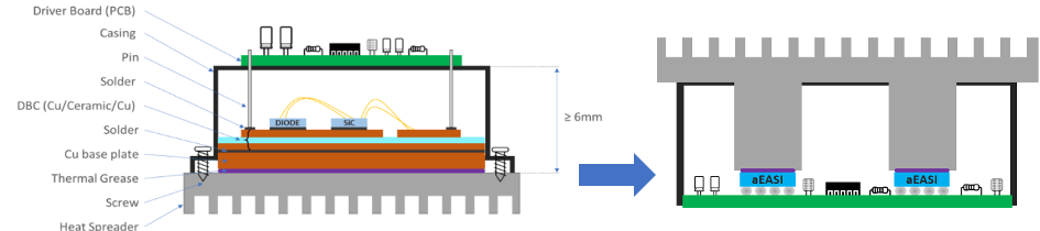
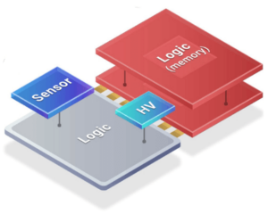
Are new packaging technologies needed to answer automotive electronics market needs? Not according to ASE’s Jean-Marc Yannou. In his keynote, he noted that similar to 5G and other demanding markets, rather than developing revolutionary technologies for automotive electronics, OSATs like ASE are working on packaging evolutions. For example, they are moving from well known, simple and trusted technologies like printed circuit board assembled (PCBA) electronics of discrete devices and high-reliability lead frame packages to 3D and SiP high-reliability packages that are ready for higher power, such as ASE’s proprietary advanced Embedded Active System Integration (aEASI) embedding technology (Figure 1).
“But reliability incurs costs and slows innovation down”, explained Jean-Marc and discussed possible solutions: “Higher Reliability can be achieved with avoidance of contaminants by using higher class clean rooms (below 1K) and dedicated lines for ATV, avoidance of human errors and manipulations by using automated lines or dedicated staff, more inspection, higher reliability materials. But to justify these investments, high volume runners are needed.”
Cost and Yield Are Key
In her presentation, “Cost and Yield Considerations of 2.5D and Fan-out on Substrate Technologies” Amy Lujan, Savansys, compared chip-on-interposer-on-substrate (CoIoS) and fan-out on substrate (FOoS), as both support HBM designs. Her analysis showed that FOoS Fan-out on Substrate will always be more cost-effective because it does not have an interposer, which is an extra and expensive part of the 2.5D design. Customers need to check the fulfillment of technical requirements, as both perform differently. However, the yield is a key factor for both technologies. “Not only will expensive processing be lost to scrap, but expensive logic dies and memory stacks too,” she stated. Large substrates are a key component to the overall package cost, as substrate might be 20% to 50% of the total package cost.
Highly Integrated 3D-SiP in The Market
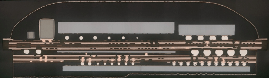
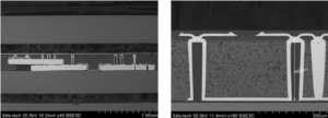
Now available on the market, 3D-SiPs including SiPs in mobile for advanced RF technology, wearables, and RF front end modules; AiP in mobile for mmWave; and FOWLP/FOPLP in mobile for side-wall-protection (PMIC using Deca M-Series process) have been reverse-engineered and analyzed by the electronic costing and technology experts at System Plus Consulting (Figure 2). CEO, Romain Freux presented the company’s findings. As always, those cross-sections are very high quality, and engineers, of course, love to see what’s inside.
Romain summarized that across its application space, SiP is a mature platform with a cost advantage linked to simplification of system bill of materials, (BOM). With face-to-face configuration or enhancement in package shielding, SiP is well fitted for RF modules with strong possibilities of miniaturization and cost reduction. MmWave packaging is a mature platform. The technology management is well known at a larger scale (e.g. automotive and industrial). As usual, the aim is to reduce the packaging in order to fit in the consumers’ devices.
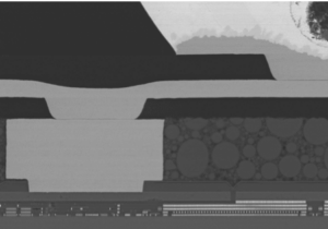
As an example of FOWLP/FOPLP in mobile for side-wall-protection, productive HVM samples of Qualcomm PMIC manufactured using Deca’s M-Series process were analyzed (Figure 3). They show superior reliability on board-level and better results in crack and drop tests compared to other FOWLP/PLP technologies.
Longtime Path for Semiconductor Integration
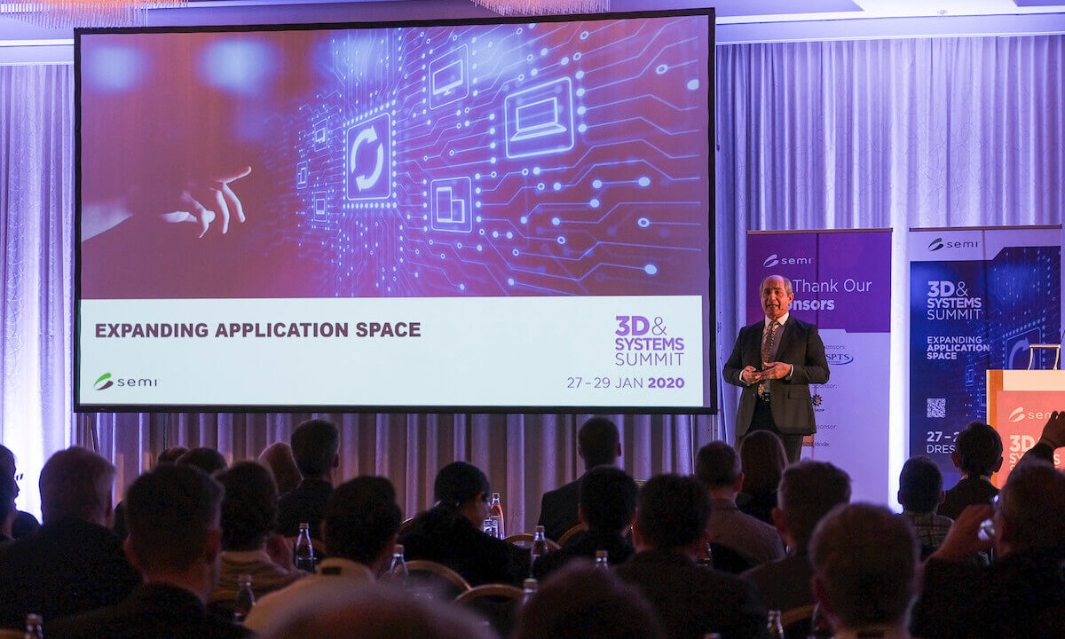
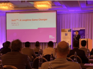
The presentation most anticipated by the majority of the attendants was the strategic keynote “SoIC™ – A Longtime Game Changer” given by Dr. Douglas Yu, VP of Integrated Interconnect & Packaging of Taiwan Semiconductor Manufacturing Company Ltd. (Figure 4). The steering committee and the organizers were honored to welcome Yu to Dresden as a keynote speaker, despite the fact that Chinese New Year – 2020 Year of the Rat – makes it difficult for our Asian colleagues to attend the summit.
Doug presented system on integrated chip (SoIC™) as a new technology, which he said is an important addition to TSMCs’ WLP and a strategic longtime path for semiconductor integration. He called it a holistic approach to the heterogeneous integration technology (HIT) platform. It helps to achieve the target by creating a new heterogeneously integrated SoC with SoC-like performance out of functional chiplets of a disintegrated SoC.
Backend heterogeneous integration (BE-HIT) will continue, and with new fine-pitch, high-density, short-path interconnects, so-called 3D interconnect density (3DID) front-end heterogeneous integration (FE-HIT) will be enabled.
“Moore’s Law will not stop: Moore’s Law 1.0 is SoC 2D scaling, which is slowing down, but Moore’s Law 2.0 is system-on-package (SoP) 3DID scaling. HIT drives the cost/ function down.” Yu explained. “That way we will continue with 2x density (3DID) increase every 2 years.”

TSMCs’ CoWoS® commercialized chiplet HIT in 2012. WLSI BE-HIT technologies offer a broad technology portfolio for chiplet integration using a bonding migration path: C4 (FC) ~120/mm² → µBump (3DIC) ~800/mm² → Bump-less (SoIC™) 12.000 to 1,200,000/mm². The holistic HIT starts the new HIT era: Frontend HIT + Backend HIT.
The SoIC™ is a disruptive 3DIC that enables the closest proximity between integrated dies, very small bond pad pitch down to below 10um and good scalability (Figure 5).
What does SoIC chiplet stacking look like? The bottom die is active side face-up, the top die is active side face-down, F2F interconnection, TSVs in the top die are revealed by wafer backside thinning of the top die. BGAs on the backside of top die connected to active sides of both dies via TSVs. The SoIC™ with multi-layer stacking will allow for the ultimate near-memory-compute.
The path Yu described is 2.5D → 3DIC → SoIC™, from chiplets to deep-partition for long-term system integration with re-use of partitioned design IP and legacy technology. 2.5D Integration and 2.5D + 3D Integration path: SoC → Chiplets → deep partition. He reminded us that while 2.5D is simple, it consumes Si area and compromises bandwidth and latency. There is better power efficiency and bandwidth for a lot of IC functions on-chip. The vision is SoIC™ for deep partition.
An important note from the Q&A session: TSMC will not change to panel format, not because they don’t like it, but they are more familiar with wafer processes. FE-HIT requires semiconductor equipment, processes, and manufacturing environment, as it is similar to BEOL in the wafer fab. TSMC can leverage wafer fab for fine-pitch system scaling and existing OIP ecosystem, technology supply chain and EDA. SoIC™ is for frontend and round wafer, leveraging FE equipment, processes, and knowledge.
Alternative 3D-Interconnection and TPV
The presentation with the longest title: “3D-RDL and Conformal High Aspect Ratio Pre-formed TPVs for RDL-First Type FO-Packages: Enabler of Advanced 3D Wafer-level System Packaging for 5G Applications” was given by Ayad Ghannam, CEO and Founder of 3DiS Technologies, France.
5G RF frontends require SiP technology and 3D integration to enable more RF bands in smaller package form factor. 5G SiPs require backside interconnects or double-sided RDL for e.g. package-on-package (PoP) integration, antenna-on-package (AoP), creation of RF feeds for interfacing with an antenna array.
Bringing the contacts to the package backside requires thru-package-vias (TPVs). Those can be produced either post-formed e.g. by laser ablation in mold compound and filling with metal, or pre-formed e.g. by the placement of PCB-Via-Bar in package or electroplated using large Cu pillars before molding.
Current TPV solutions are either not easily compatible with backside RDL or require a high number of process steps – increasing complexity for different height TPV in the same package – and are in general costly. The newly proposed low-cost pre-formed high aspect ratio (HAR) Thru-Package-Vias (TPVs) using 3D-RDL technology e.g. for 3D stacked RF system has been successfully demonstrated by 3DiS Technologies in collaboration with the company Ampleon, an early adapter of the 3D-RDL technology (Figures 6 and 7). The main features of HAR TPVs are: Height of 270µm, Diameter of 45µm and aspect ratio of 6:1.
3D-RDL enables ultra-thin 3D-FOWLP and 3D-WLSiP, both RDL-first, face-down and/or face-up type) e.g. for RF applications. Coupled with pre-formed HAR TPVs, it allows for bringing contacts to package backside by a low number of process steps. It enables 3D integration inside the package with short 3D interconnects. Reliability tests show very good results at both, package and board-level. It’s an innovation to advanced 3D packaging of 5G applications. 3DiS was presented with the 3D InCites Process of the Year Award for this technology.
The Next 3D & Systems Summit
Stay tuned for the 3rd edition of the 3D & Systems Summit, which takes place January 25-27, 2021, again in the center of breathtaking ancient downtown of Dresden, Germany. The summit venue, Dresden Hilton Hotel, is located just in the opposite of Frauenkirche at Neumarkt, a unique 3D-Baroque masterpiece built 1726 – 1743, destroyed in the firestorm of February 1945 shortly before the end of WWII, rebuilt 1994 – 2005 and today a world-known symbol for peace and conciliation.