Latest Posts
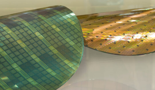
aveni® S.A. Announces Breakthrough Electrical Yield Results for 12:1 Aspect Ratio TSVs
MASSY, France – Jan. 23, 2018 – aveni S.A., developer and manufacturer of market-disrupting wet deposition technologies and chemistries for...
Heterogeneous Integration enabled by Advanced Packaging Leads the Way at SEMICON West 2016
I have to admit, after attending this week’s SEMICON West 2016, I’m feeling a little smug. Why? Because after years...
3D/TSV Officially Recognized as Advanced Manufacturing Technology at SEMI ASMC 2016
As Dick James, Chipworks, puts it, the SEMI Advanced Manufacturing Conference is “… an annual conference focused on the manufacturing...
ASMC 2016, the Return of MEPTEC Luncheons, and Your May Calendar
The Saratoga Springs, NY, horse racing season starts in late July, following a racing tradition that dates to the 1860s....
Cost Analysis of a Wet Etch TSV Reveal Process
Through silicon via (TSV) technology is a key design element being incorporated into more and more advanced packaging designs today....
In Conversation with Yann Guillou About the SEMI European MEMS Summit 2015
Yann Guillou, Membership & Business Development, SEMI Europe, talked with 3D InCites / 3D+ about the upcoming European MEMS Summit...
ASMC 2015: Has the Wonderment of Semiconductors Become a Presumption?
The 26th annual SEMI Advanced Semiconductor Manufacturing Conference was held in Saratoga Springs, NY, May 3-6, 2015. ASMC 2015 drew a...
More Spoor: Heterointegration in the 2015 Analog, MEMS and Sensor Startups to Watch, Part 2
In Part 1 of this series I drew your attention to what Peter Clarke, writing in EETimes on 02 January...
The X-ray Metrology of TSVs and Wafer Bumps
Being able to look inside an object without opening it up or destroying it, and separating the different features within...

Riding Out on a Horse and in on a Goat: 3D IC Predictions for MEMS
The Lunar New Year is soon upon us, and we will be celebrating the Year of the Goat with firecrackers,... Understanding Heterogeneous 3D Integration
“How is heterogeneous 3D integration defined?” There are certainly different understandings in the microelectronics community regarding the definition of heterogenous...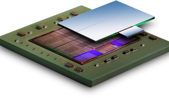
GIT 2014: “Call them Interposers, as God Intended”
Subu: “I find the whole concept of 2.5D fairly atrocious. I have banned its use.” Rao: “what are you going...
A Path Finding Based SI Design Methodology for 3D Integration
3D integration is being touted as the next semiconductor revolution by industry. 3D integration involves the use of various interconnects...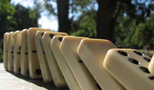
The 2014 European 3D TSV Summit: Get Ready for the Domino Effect
I just boarded my flight home after attending the 2014 European 3D TSV Summit. Three days, 332 attendees from 21...
Launching a Trillion Sensors on a Sea of Through Silicon Vias
To the readers of 3D InCites: Happy New Year! I hope your 2014 will be a healthy and prosperous one...
Successful 2.5D Test Vehicle Project Launched by GLOBALFOUNDRIES, Open-Silicon and Amkor Technology
GLOBALFOUNDRIES has unveiled details of a 2.5D test vehicle project that demonstrates the value of its open and collaborative approach...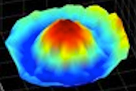
Rudolph Technologies’ Metrology, Inspection and Lithography Solutions for 2.5D and 3D TSVs
Here’s one thing the team at Rudolph has a firm grasp on: understanding that feature sizes of today’s wafer-level, 2.5D... SPTS Ships 1000th DRIE Process Module
Milestone shipment extends company’s leadership in DRIE Newport, United Kingdom, and SEMICON Singapore, 7 May, 2013 – SPTS Technologies, a supplier...