
I just boarded my flight home after attending the 2014 European 3D TSV Summit. Three days, 332 attendees from 21 countries, 24 presentations, 3 keynote speakers, 2 panel discussions, several face-to-face interviews and lots of side conversation all about 3D TSVS being Application Ready leads to a good deal of information to process and write about. So let me start off with some key take-aways and general observations.
Overall the market forecasts really didn’t reveal anything earth-shatteringly new. In his Supply Chain Market Forecast, Mark Stromberg, Principal Analyst Gartner, noted that the economic concerns that are limiting the TSV ramp should be resolved by late 2014-2015, but thinks the number of companies that will implement TSV technology will be limited due to capital costs issues and “macro-based concerns.” I’m not sure I agree with that prediction, but only time will tell. He also said that as we move to the 10nm node, TSV becomes a required technology for system design. (That was particularly good news). The next “killer app” will be wearable devices and the Internet of Things.
Overall, I would say the key takeaways from this conference at the highest level concerned manufacturing readiness (we are, except for thermal management), cost-of-ownership (we’re working on it and there is progress in these areas) and how much longer is it going to take (this depends on your definition of IT.)
It’s been established that the manufacturers have everything they need in place to start running product when the system architects start designing in 3D devices. But they’re also all smart enough to not put all their eggs in one basket, and all of them talked about different offerings to address latest design requirements. The overarching point is, all of these will coexist and serve the diverse needs of customers.
TSMC clearly sees the writing on the scaling wall. According to Mei Kei Ieong , VP Technology, TSMC Europe, the company knows that the end of traditional CMOS scaling is imminent, and as they are in the business of selling wafers, if the customer calls for 3D ICs, they’re going to give them 3D ICs. Or 3D TSV wafers. Heck, they’ll even give them fan-out wafer level packages (FoWLP). They will provide end-to-end services, or will collaborate with OSAT partners. Whatever it takes to stay at the top of the heap.
Ieong’s keynote was titled “A New Paradigm – System Scaling through 3D System Integration.” His message – TSMC has always been an innovator in materials and a leader in providing higher performance technologies. They have a robust More than Moore portfolio with leading-edge 3D transistors. He talked about a 3D IC design paradigm TSMC calls “through transistor stack” using TSVs to enable heterogeneous vertical scaling. He also talked about the CoWoS process (chip on wafer on substrate), where die are placed horizontally on top of the interposer. The advantage of this, he says, is that the dies on top don’t need TSV processing. All the TSVs are done in the interposer.
TSMC has demonstrated Wide I/O DRAM — that’s JEDEC standard for Wide I/O 2 for High Bandwidth Memory (HBM) — using CoWoS. The tapeout plan is to validate HBM on CoWoS. The company has also demonstrated vertical stacking of memory on 28nm logic device for mobile applications. And for those who want a cheaper alternative to CoWoS, TSMC introduces InFO-WLP, qualified for production, with better thermal performance, smaller form factor than CoWoS, and cost competitive to flip chip.

Offering GLOBALFOUNDRIES’ readiness update, Michael Thiele said the company has a TSV line installed in its Malta facility, and that it has TSV integration characterized for 20nm, and 14nm is on the way. The bump and test facility is under construction.
Thiele offered reasons why commercialization of both 2.5D and has and is taking so long: The technology took longer than expected; the need for players to see the return on investment (ROI) before making a commitment; and identifying the right applications. “2.5D is not a decision they made for one product. It’s a platform decision,” he explained, “and making the wrong decision can have severe consequences.” Additionally, improvements to existing technologies have extended the need to adopt TSVs.
The most significant part of Thiele’s talk was the three customer trends he described, with regard to adopting 2.5D and 3D integration.
- Trend 1: The end customer does not accept the price increase, even though the performance is significantly improved. There will be niche introduction to 2.5D until the cost comes down significantly. Instead, the trend is to extend the lifetime of existing packaging technologies.
- Trend 2: The end customer plans to introduce a 2.5D product in an application space that is in a high-end market sector that accepts a premium price for the product.
- Trend 3: The end customer introduces 2.5D and 3D to reduce system cost. They use same-node partitioning to gain the yield benefit (think Xilinx, but there are others less publicized) compared to large SoC. To minimize scaling cost impact, they use it to implement mult-node approach. OR to avoid the transition to mult-patterning lithography to achieve smaller Si nodes, they use 2.5D integration to improve system performance.
Whatever the trend, Thiele says GLOBALFOUNDRIES is ready. Design systems, design rules and PDKs, etc are available now. The supply chain is in place. Thiele says he expects GLOBALFOUNDRIES will be ready to support customer demand in the second half of this year.
Reporting on behalf of STATS ChipPAC, keynote speaker, Raj Pendse declared, “The application is not ready, but we are ready.” He said that over the last 5-10 years, I/O density has grown rapidly and he sees parallel fronts emerging in the 3D space. He says that package stacking is plateauing. At the wafer level, he sees growth in thick-film based technologies such as fan-in and fan-out WLP. The highest-level density available is Si level TSV, and there is a convergence moving toward Si. Pendse also made a case for Si partitioning on 2.5D interposer, saying that there’s approximately a 16% impact expected for large Si die, and it may be viewed as equivalent to the new Moore’s Law trajectory. “By breaking (the die) into four parts, you cover the cost of the interposer and the package value goes down,” he noted.
He also divided the drivers for packaging solutions in to “logical groups of density”. Group one is fab-based, Si TSV such as CoWoS; Group 2 is Si/glass/organic interposer and FOWLP. Group 3 is conventional laminate build up.

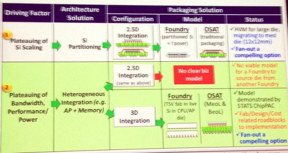
On the topic of business models, Pendse showed the following chart indicating that viable models exist for 2.5D monolithic Si partitioning and 3D heterogeneous integration, but that 2.5D heterogenous integration lacks a viable business model. He also noted that FOWLP is a “compelling alternative for both 2.5D and 3D integration.”
As far as STATS ChipPAC readiness for 3D integration, the company, in collaboration with UMC, qualified Wide I/O memory on a 28nm vehicle last January (2013), He walked the attendees through the individual process steps to get there, including such details as refinement of fine-pitch Cu pillar bumps with elliptical bumps. “As a company we are ready,” he noted. “Our counterparts are ready.”
Rather than focus on Amkor’s readiness, Ron Huemoeller, Sr VP Advanced Platform & Product Development, provided an interesting perspective on 2.1D (what is that? We’ll get to it in a second) and 2.5D, and how there is room for both in the market. “Once you design in a package and its qualified, it doesn’t go away,” he noted.
The differentiator between 2.1D and 2.5D is the presence of TSVs and the interposer material. Therefore, 2.1D is merely an advanced multichip module on an organic substrate – often a highly integrated organic interposer. This technology is substrate supplier driven, and is limited to 2-6µm line and space requirements.
2.5D uses TSVs, and the interposer is either silicon or glass mounted on an organic substrate. Any package platform with <2µm line and space requirement calls for Si interposer. Huemoeller says the market is split between high, mid and low end for 2.1D and 2.5D and that the high end will need the Si interposer. Furthermore, he said 2.5D is impacting the organic substrate suppliers are aggressively addressing this. Designing into Si and out of organics simplifies the motherboard.
On the topic of cost for 2.5D he offered this advice: “You don’t have to have the same prices as current packages, but you need to be in the neighborhood. If you’re close enough, the market will go.
“We believe that 2.1D has tremendous opportunity in the mobile space,” he said. “2.5D needs to depend on routing….Substrates have a tremendous opportunity there.”
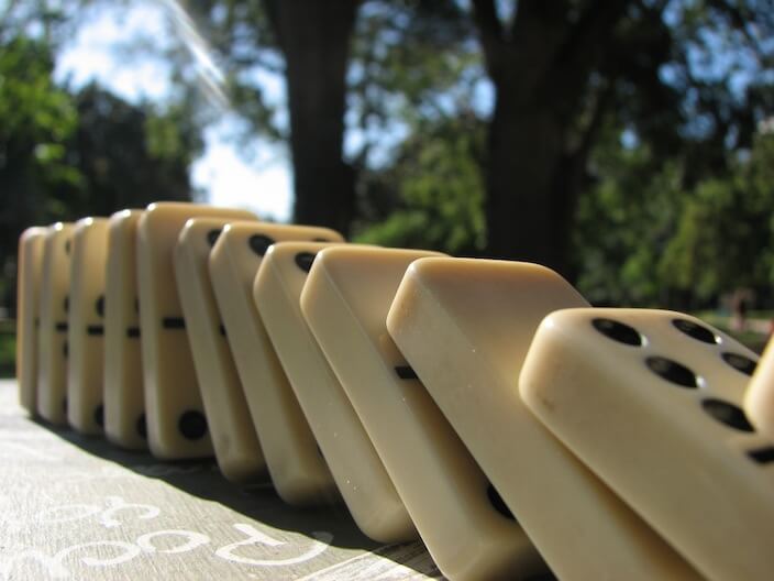
Knocking Down the Dominos
Probably one of the most significant take-aways from this event was Huemoeller’s domino analogy. Nobody leaves his or her driveway going 100 miles an hour. 2.5D is here. TSV used in heterogeneous integration for high-end medical devices and MEMS 3D is here. The rest is coming, and the momentum is building. Xilinx Virtex 7 was the first domino to topple, but Huemoeller says it wasn’t a big enough to make a wave in the market. He says Amkor thinks graphics players are big enough. It will become a race and everyone will design it in, and that’s when domino effect will really get going. All it takes is one. Who’s it going to be? ~ F.v.T.


