
Wafer Thinning and Nano TSVs
In the last few years, Ann Jourdain of IMEC and co-workers have described silicon device stacking through extreme silicon thinning technology.
Recently Jourdan and Dave Thomas of SPTS reviewed this technology for the Jan/Feb issue of Chip Scale Review. The technology is interesting enough that IFTLE will take a closer look at it.
Via-last through-silicon vias (TSVs) are typically used to connect the backside to the front side of a device wafer through several microns of thinned silicon. For submicron interconnect pitches the thickness of the silicon must be reduced to keep the TSV aspect ratio to < 10:1, which is a normal range to allow subsequent oxide and metal depositions. Nano TSVs (defined here as oblong 180 x 250nm diameter TSV in 500nm thickness silicon) would require silicon thicknesses of < 1µm. This is depicted in Figure 1.
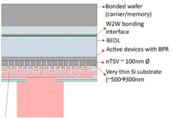
To reach sub-500nm interconnect pitches, via-last TSV scaling a sub-micron wafer thinning process was developed that enables a very tight thickness control over the entire wafer, with less than 70nm total thickness variation (TTV), and nano TSVs were etched using a Bosch process applied to extremely small CD structures (180x250nm top CD).
Thinning to 5µm can be achieved by a combination of grinding, chemical mechanical planarization (CMP), and dry etching. In order to achieve the desired sub 1µm thickness with acceptable total thickness variation (TTV), they have found that an embedded etch stop layer is required. They have achieved this by first growing a 50nm SiGe layer on a 300mm wafer and then capping that with 500nm of silicon. That silicon serves as the surface for device fabrication.
After the devices are formed, this device wafer and a carrier wafer are face-to-face bonded through SiO2/SiCN surfaces. After wafer-to-wafer bonding, the device wafer backside is thinned by the techniques shown below.
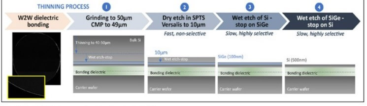
The wafer is then thinned by grinding down to 50µm. Grinding damage is then removed by 1µm of CMP. The next 39µm of silicon is removed with dry etching leaving 10µm above the SiGe etch stop layer. A wet etch is then used to remove the remaining 10µm of Si and stop on the SiGe layer. The SIGe is then selectively chemically-etched to expose the 500nm epitaxial silicon layer.
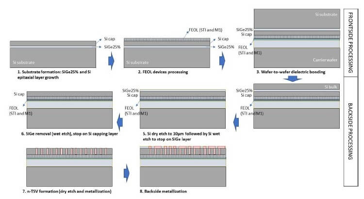
Forming nano TSVs involves Bosch etching (They reported that Bosch etching was more stable than ICP etching) and stopping above M1 and the subsequent deposition of 10nm of PEALD SiO2 lining the TSV. The TSV and M1 liners are then etched to expose M1. The TSVs are then lined with TiN and Cu seed, plated with Cu and CMPed. A single damascene layer then completes the backside metal.

Making Money on the Leading Edge
The recent data released by IC Insights indeed shows the economic effect of TSMC leading the pack when it comes to leading-edge front-end chip manufacturing.
As we can see in Figure 4, TSMC, which has always been at the leading edge, and always led the pack when it came to revenue per wafer, took a jump in 2018 and is broadening its lead over the competition. Not so coincidentally, IFTLE thinks, 2018 is when Intel got stuck attempting to move to 10nm (which is where they still are ) [see IFTLE 458 and 470]. Even though they are not really competitors, Intel falling behind had/has a significant impact on community psychology.
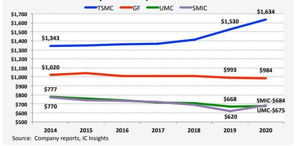
TSMC is the only pure-play foundry manufacturing ICs at both 7nm and 5nm process nodes. Not coincidentally, its overall revenue per wafer increased significantly as many of the top fabless IC suppliers lined up to have their newest designs manufactured using these most advanced processes nodes. As IFTLE has repeatedly stated, Samsung is now the only player attempting to keep up with the TSMC juggernaut.
For all the latest on advanced packaging stay linked to IFTLE………………


