

In Part 1 of this series I drew your attention to what Peter Clarke, writing in EETimes on 02 January 2015, called the “15-in-15: Analog, MEMS and sensor startups to watch in 2015.”
What would we find if we were to look for signs of heterointegration in this particular gathering, I asked?
And what did we find when we looked for heterointegration spoor amongst these first 5 of Peter’s 15 notable startups?
The companies profiled in Part 1, namely Cambridge CMOS Sensors; Chirp Microsystems; Dual Aperture International Co. Ltd; Dyna Image; and Gpixel Inc, the first “5-in-15”, intrigued me enough to want to go back to Peter’s watering hole for this second round, as the tracks of heterogeneous integration were heavy on the ground the first time we looked.
Keep close, mind your trail manners, and let’s take an in-depth look at the middle 5 notables.
Hanking Electronics started the Hanking Micro-Electro Mechanical Sensor Industry Park project in February 2011, in Shenfu New Town, in the Fushun Development Zone, Liaoning, China, to bring 200mm high volume MEMS manufacturing to China, for the Chinese market place in the consumer, automotive, industrial and medical markets. Hanking Electronics is part of the Hanking Industrial Group, whose other businesses include mining, metallurgy, commerce and precision manufacturing.
In other words, they think big.
Hanking’s business model? “The [Hanking] MUMPS China process gives users access to proven MEMS process and wafer fabrication facilities at a fraction of the price of traditional MEMS foundries.” (MUMPS = multi-user shared MEMS process.)
Why MUMPS China? “To get more internal Chinese fabless MEMS companies started, growing and working their way through the MEMS development process,” according to Doug Sparks, executive vice president, Hanking Electronics, in his talk at SEMICON West 2012.
 And the heterointegration angle at Hanking? None that I could find, at least for now. Although the Ring of Life structure in Shenfu New Town does have a certain … je ne sais quoi.
What is QuantumFilm technology? According to InVisage, next on the list today, “QuantumFilm was designed to absorb 100% of the light we see with our own eyes and do so in a film whose thickness is measured in nanometers. We took the magic of photographic film — that captures memories that last us a lifetime — and integrated it intimately onto a silicon chip. … This translates into spectacular images in any lighting condition, and an incredible sharpness of detail and color that recalls your Hasselblad.”
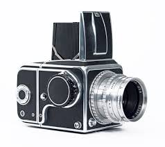 Ah, my old Hasselblad …
As Colin Johnson wrote in 2010, QuantumFilm is “made from materials similar to conventional film—a polymer with embedded particles—instead of silver grains like photographic film the embedded particles are quantum dots.” The QuantumFilm is painted “… atop a low-cost wafer that has the electrode array for super-dense high-pixel-count images, but without any of the expensive CMOS photodetectors that make up the bulk of conventional digital camera sensors.”
A quantum dot-embedded polymer film atop a silicon chip? Score one for heterogeneous integration, courtesy of InVisage. Your Hasselblad is jealous.
And from the photonics / image sensor side of the house there’s even more to hear, this time from our third player, ISORG. What does ISORG do? “ISORG converts plastic and glass surfaces into smart surfaces,” offering “a new generation of high performance opto-electronic sensors with 3D product integration capability recognizing any shapes and form factors.”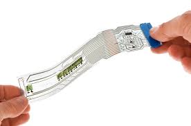
The ISORG process is “compatible with system-on-foil integration (co-integration of printed sensors with discrete components and integrated circuits on plastic).” Current manufacturing is being done on the ISORG pilot manufacturing line, Grenoble, on 32cm x 38cm plastic foils; a mass production demonstrator is planned for 2015-end, on 60cm x 70cm plastic foils.

Co-integration of printed sensors with discretes and ICs on plastic? Heterointegration, loud and clear, even if the plastic substrate throws your silicon-centric thinking for a loop. Heterointegration scores again. We are two for three.
Linx Imaging extends the run of startups to watch in this segment, again a startup working on image processing, advanced sensor and optics technology.
Linx seems to be something of a cypher; after a brace of press releases in 2014 about Linx aiming to put SLR image quality in the pockets of consumers, some of the links embedded therein are now dead-ending, and the trail of the Linx is running a little cold. No fresh spoor here.
The fifth and final company today is mCube Inc. Peter Clarke’s dead giveaway about mCube and heterogeneous integration in his January piece is this: mCube “has developed a method for integrating MEMS motion sensors above electronic circuitry in a standard CMOS wafer fab using through-silicon via connections.”
 It’s monolithic MEMS on CMOS IC. Advantages of this monolithic approach by mCube are said to be smaller size, higher performance, lower cost, and the ability to integrate multiple sensors onto a single-silicon chip.
Heterogeneous integration? Monolithic integration of MEMS and CMOS as described by mCube is heterogeneous integration in my book.
You can read more about mCube’s process in a good white paper they have available for download, and you should probably also know that mCube secured three awards at the MEMS Executive Congress US 2014, including the award for MEMS Start-Up of the Year.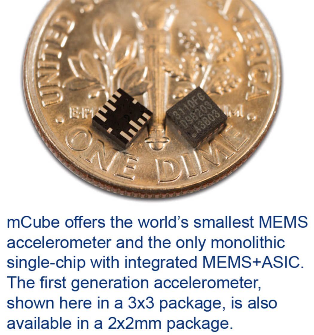
Now that’s a hot start-up. And a good boost for heterointegration.
And a good place to end our hunt for heterogeneous integration spoor in the middle 5 of the “15-in-15.”
Final count: 3 heterointegration sightings within the 5 companies examined here, with mCube making a clear case for heterogeneous integration’s advantages in the world of smaller-faster-cheaper-better.
Peter, again, thank you for giving me a launch pad for these pieces. And from Pittsburgh, PA, readers, thank you for reading. ~PFW


Comments are closed.