

Did anyone miss the Sound of Music bit during the Oscars? Anyway, with the sounds of “The Hills are alive..” in my head, I drove off the next day down to the Hill Country in Austin to the invitation-only, On The Road to Fine Feature IC Package Substrates and Interposers Workshop, hosted by Jan Vardaman of TechSearch International.
This is a nice, comfortable-sized venue with approximately 100 attendees that makes for some very interesting one-on-one conversations.
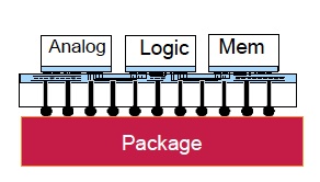
“Sixteen Going on Seventeen” : You cannot go to a 3D packaging seminar and not see a presentation on the Xilinx interposer package. So aptly, Ivor Barber of Xilinx updated us on the Xilinx perspective. Xilinx prefers to refer to the interposer as Stacked Silicon Interconnect Technology (SSIT). Clearly, Xilinx business being FPGAs related to the issue of large die cost. Larger dies have lower yield, and by partitioning the large die into four smaller dies on the interposer, cost-reduction is achieved with minimal performance impact. From Xilinx perspective, going down an SOC route is economically less attractive than the going to interposers. Why? In a mix of logic, memory and analog, the different technologies scale at different rates, and the costs are not optimized. Xilinx is planning newer packages based on TSV will that will take it from the teen years to maturity.
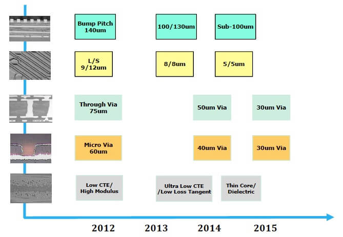
“Sound of Music” : Chaowen Chung from Unimicron and Susan Bagen from Endicott provided updates on trends in the laminate space. Chaowen showed Unimicron’s roadmap for heading to finer pitch capabilities, while Susan showed the need to accommodate stresses created due to die and board interaction and PCB design needed to support bare die placement. Clearly the laminate folks are eyeing the interposer space as a possible opportunity. Chaowen clearly stated the need to implement steppers to achieve the fine pitch. This was sound of music to my ears as Rudolph Technologies has just entered the advanced packaging stepper business.
“Do-re-mi”: Osborne Martin of Intel talked of the metrology Requirements for Fine Feature Organic Substrates. Basically, finer line width is driving the increased need for inspection and metrology. He emphasized that metrology is usually considered non-value added. For Intel, it has enabled deployment of fine-feature substrate based packages. As Rudolph does a lot of back-end wafer level inspection, any topic on metrology strike some chords deep down.
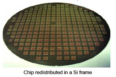
John Hunt of ASE, Shigenori Sawachi, J-Devices Corporation and Ted Tessier of Flip-Chip International showed how the FC-BGA is evolving into fan-out wafer level packaging and embedded die in PCB alternatives taking advantage of advances in laminate technology. The most well known example of fan-out WLCSP is the eWLB package; which is die re-constituted as a wafer in some form of “plastic” material. John showed the embedded die in silicon as well as embedded die in PCB as variations on fan-out packaging. Talk about Inception (the movie) in the silicon world, where you singulate the die from a wafer and then put it back into a SI wafer to re-form the wafer and fan-out using RDL. Sawachi-san talked of J-devices jumping straight to panel-level processing for their version of fan-out WLCSP and the cost advantage of using PCB type processing equipment to show cost-advantage. Ted showed an FCIC-Fujikura collaboration on die on a flex-circuit fan-out approach.

“Edelweiss” : Micheal Heise of IPDiA, based near the French Alps, showed how embedding capacitors in the interposer could provide the highest capacitance density in silicon by taking advantage of the depth of the vias in Si to provide a bigger area for increased capacitance.
Sesh Ramaswami, of Applied Materials, pointed out some of the cost break-down that goes into Flip-chip. The top three being Cu dual damascene, Front side pad finish and backside bump, followed by litho for Cu dual damascene. The cost structure generated quite a bit of exchange. However, the best take way would be the relative costs of each process and percentage contribution to the overall cost as opposed to the absolute. He rather boldly stated that development issues for 14nm Cu pillar is complete and the platform is ready for more advanced nodes.
“My Favorite Things”: The best part was the panel discussion with Ron Huemoeller of Amkor, Ivor Barber, John Hunt and Michael Su of AMD on their perspectives on 2.5D. Some interesting questions were posed and lot of good discussion regarding both the effects of this warped die on substrates and direction of interposer.

“The Lonely Goatherd”: The first big question – glass versus silicon interposers? It became evidently clear that glass may occupy some form of a niche, but most of the OSAT companies has investment and experience in Si processing and more than likely 300mm Si Interposer is going to be the main interposer material. Glass as an interposer is probably the lonely goatherd. The eWLB was also offered as an interposer platform. After all, you can add dies on top of the package and connect them to the embedded die with vias and RDL.
The second big question – When do you expect HVM for 2.5D other than FPGAs? What’s the next application? This turned out to be a more difficult question to answer. No one offered any clear answer. I suspect CDAs are in place.
“Climb Ev’ry Mountain” : The third big question – what drivers do you see that would accelerate TSV into HVM? This was easy to answer. Cost. Totally unanimous. Significant cost reduction is required to get TSV as an enabling technology for 3D packages.
“No Way to Stop It”: What became clear is that we are entering an era of collaboration up and down the supply chain. It is not enough for the OSAT to be working in vacuum from either the foundry or the EMS folks. Ron Huemoeller explained it clearly with an example. The opportunity is in bringing in the interconnect onto the interposer to reduce latency, improve performance and perhaps simply the PCB and reduce the metal layers. Should we be calling this “interconnectology”? hmmm… This a system integration approach to packaging and no doubt reflects the collaborative business model of the future – no way to stop it.
“So Long, Farewell”: Jan showed an excellent time-line of interposer development, courtesy of Xilinx. We forget how long it takes for development. Xilinx started development of interposer back in 2006. The original test vehicle for the Xilinx interposer was in 2008 on a 90nm process. The first real product did not come out till the 28nm node in 2011. A good 6 years from the initial development. So as we went back to our work-places and pace the development within our own companies, it’s good to keep time whole time-line in perspective. ~ R. Roy


