


3D: The El Dorado of Heterogeneous Integration
From the cloud to edge computing, the quest for ever-greater power efficiency remains researchers’ top priority. From high-end niche to mass-market applications, the best cost-to-performance tradeoff is key to providing a competitive advantage. While Moore’s Law has helped meet the performance required in terms of data transfer and power efficiency...
CEA-Leti/Intel Collaboration brings 3D Powerhouses to the Advanced 3D Packaging Table
CEA-Leti and Intel recently announced a new collaboration effort on advanced 3D packaging technologies for processors to advance chip design. The research focuses on the assembly of smaller chiplets optimizing the interconnect technologies between the different microprocessors and on new bonding and stacking technologies for 3D ICs focused on high-performance...
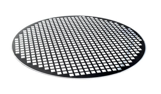
Plasma Treatment During Fan-Out Packaging Maximizes Performance and Optimizes Costs
In recent years, there has been an increased focus on fan-out wafer-level packaging (FOWLP) due to the smaller packaging size requirements for smartphones and handheld electronic devices. FOWLP – and fan-out panel-level packaging (FOPLP) – is the process during which known good dies (KGD) from the original silicon wafer are...

48V Ecosystem and Power Packaging Trends
With each passing year, emerging growth application areas such as Automotive, Cloud Computing, Industrial Automation, and Telecom (5G) Infrastructure are garnering more attention. Although the application segments are different, there is a commonality in how voltage conversion and power distribution are achieved at the system level. System demands are becoming...
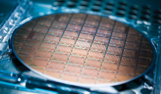
Carrier Wafers for Semiconductor and MEMS Manufacturing
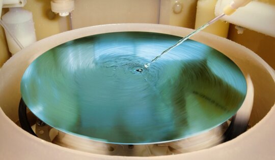
As technology rapidly moves forward, the reduction of device and chip size is playing an important role in implementing as many chips and sensors in the smallest space. For this reason, the thickness reduction of semiconductor wafers is necessary. Thin semiconductor wafers (thickness around 50-100 µm) are flexible and fragile....
Temporary Wafer Bonding System Is Based On Electrostatics, Not Adhesives
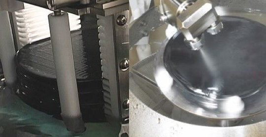
Temporary wafer bonding is widely employed in semiconductor device fabrication and in semiconductor device packaging applications, particularly now that changes in the Z dimension are calling for thinner and thinner silicon devices, and thinner and thinner packaged devices. This means that wafers and singulated die must be supported through parts...
Temporary Bonding and Mold Process to Enable Next-Gen FOWLP
Temporary wafer bonding processes were initially developed for enabling three-dimensional (3D) stacked integrated circuits (ICs). For example, dies can be stacked on top of each other using die-to-wafer stacking to create 3D IC stacks. Through-Si vias (TSVs) and microbumps are used to interconnect the finished dies. These techniques require the...

A Look Inside The 3D Technology Toolbox For STCO
System-technology co-optimization (STCO) – enabled by 3D integration technologies – is seen as a next ‘knob’ for continuing the scaling path. In this article, we will unravel the STCO principle, open up the 3D technology toolbox and bring up two promising cases: logic on memory, and backside power delivery. After DTCO...
Addressing the Challenges of Surface Preparation for Advanced Wafer Level Packaging
As the semiconductor industry shifts focus from CMOS scaling to heterogeneous integration, the importance of surface preparation and wafer cleans during semiconductor device manufacturing is migrating from front-end wafer processing to back-end wafer level packaging processes. This, due to a combination of high-reliability applications, such as autonomous vehicles, 5G, artificial...

CoolCube™: More than a True 3D VLSI Alternative to Scaling
Almost four years ago, we published an article titled “CoolCube™: A True 3DVLSI Alternative to Scaling” on 3D InCites. It described the concept of stacking layers of transistors sequentially on top of each other and documented the research effort happening at Leti to develop a feasible process integration scheme and...
Replacing NMP: Are You Ready?
NMP is an abbreviation for N-methyl-2-pyrrolidone (other synonyms are 1-Methyl-2-pyrrolidone and 1-Methyl-2-pyrrolidinone) (Figure 1). NMP has proven itself as an effective and versatile cleaning agent, removing photoresist residue while leaving the surface in good shape for processing steps downstream. However, its time may be short-lived as companies strive to meet...

The Fundamentals and Early History of Quantum Mechanical Tunneling
The mid-1920’s were the miracle years for quantum mechanics. The “Old Quantum Theory” originating with Niels Bohr, had reached crisis point by the end of 1924. Wave-particle duality from Einstein and de Broglie called for something new. The great theorists, Heisenberg, Born, Jordan, Schrödinger, and Dirac, published different formulations of a new theory that were quickly shown to be equivalent descriptions of quantum...

The Triumph of Quantum Mechanics at the Heart of Solid-State Data Storage
If all the data sent worldwide each day on the internet were burned on to CDs and these were then piled one on top of the other, the resulting heap would reach Mars and back again. Much of this data is thankfully not stored on CDs but rather in much more efficient solid-state memories. And...
Integrated Solid-state Capacitors Based on Carbon Nanostructure
The constant demand for miniaturization, added functionality and increased performance of electronic devices systematically drives higher integration by adding more devices on a single chip. In addition, 3-D or 2.5-D packaging, require on-chip or in-package capacitors, not only in traditional integrated circuits but also for integrated components, possibly on interposers,...
3D Systems-on-Chip: Clever Circuit Partitioning To Extend Moore’s Law
In recent years, the technology of 3D integration has evolved into an economically interesting road. In particular, the technology is used to package the CMOS imagers you find in your smartphone, the high-bandwidth DRAM memory stacks used in high-end computing, as well as in advanced graphics cards. 3D integration allows...

The Dual-Gate Thin Film Transistor for 3D Dynamic and Flash Memory
Data is now the world’s most valuable resource. Solid-state storage of data is driving an innovation revolution built upon 50 years of progress. Here we look at the dual-gate thin film transistor (DG-TFT), an extremely versatile solid-state data storage device that can be used in monolithic 3D as either a flash...

Lam Research: SABRE 3D
SABRE® 3D is a next-generation electroplating product designed to meet leading-edge production requirements for advanced packaging applications. This product leverages proprietary front-end manufacturing technology and offers market-specific solutions for copper pillar and through-silicon via (TSV) fabrication. SABRE 3D offers industry-leading throughput along with reduced cost of consumables to enable high economic value...
Nordson ASYMTEK: Programmable Tilt + Rotate 5-Axis Fluid Dispenser
Nordson ASYMTEK’s programmable Tilt + Rotate 5-Axis Fluid Dispenser dispenses using 5 axes instead of 3. The X and Y tilt enables dispensing from a vertical position, varying tilt angles to all sides of a component and up to the top of a 3D stacked die with high precision and...
SPTS: Sigma fxP PVD with Multi-Wafer Degas
SPTS’s Sigma® fxP, is a well established PVD system used in advanced packaging applications such as UBM and RDL. It utilizes batch degas technology that can improve Rc whilst maintaining high throughputs, despite the outgassing challenges posed from the increasing use of organics, such as mold in Fan-Out WLP. Testimonial...
KLA-Tencor: CIRCL-AP™
CIRCL-AP™ is a cluster tool with multiple modules, covering all-surface inspection, metrology and review at high throughput for efficient advanced wafer level packaging (AWLP) process control. The CIRCL-AP provides production-proven, high sensitivity monitoring capability for multiple AWLP applications including 2.5D/3D integration, wafer-level chip scale packaging and fan-out wafer-level packaging. Testimonial...