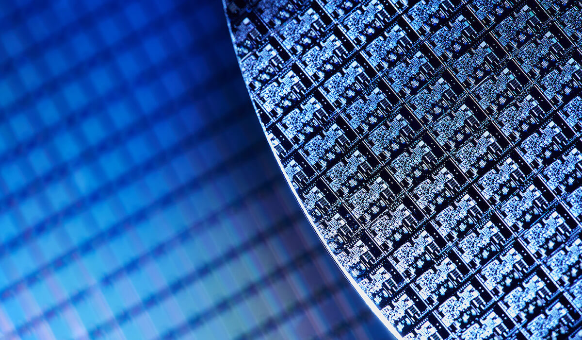
In recent years, there has been an increased focus on fan-out wafer-level packaging (FOWLP) due to the smaller packaging size requirements for smartphones and handheld electronic devices. FOWLP – and fan-out panel-level packaging (FOPLP) – is the process during which known good dies (KGD) from the original silicon wafer are selected and accurately attached to a wafer or panel-size substrate, over-molded with an epoxy compound, and then cured to create what is called a reconstituted wafer. Plasma treatment is needed to ensure that the surface is contamination-free, for surface treatment to aid the attachment process, and to remove photoresist or other organic residues.
There are two options for accomplishing the FOWLP/FOPLP process. In the mold-first option, the dies are attached to a film and then molded. Once the dies are molded, the supporting film is removed and redistribution layers (RDL) to fan-out interconnections from the die to selected regions outside the die area are formed. The second option is “RDL first”, where the redistribution layers are formed on a carrier before the dies are attached. In this process flow, a laser debonding process is used to separate the carrier from the reconstituted wafer. The final steps for both options are wafer- or panel-level bumping and singulation.
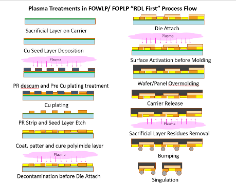
Figure 1 shows the “RDL-first” process flow and the steps where plasma treatment is needed. In this flow, the first plasma treatment is applied after the RDL patterning process to remove photoresist residues (descum process) and induce surface hydrophilicity for the Cu plating process. The next plasma treatment step is before the die-attach process to make sure the surface is contamination-free before the dies are attached. Once the dies are attached, a plasma treatment is applied in the pre-molding step to prepare and activate the surface to improve the mold adhesion, and the flow of the mold material around the attached dies. After the molding step, another plasma treatment is applied to remove sacrificial layer residues left after the debonding of the wafer from the carrier. The same plasma treatment is used for the cleaning of metal pads and lines and the removal of organic and oxide contamination to improve the adhesion of bumps to under bump metallization (UBM).
There are additional steps where plasma treatment is applied, such as in the reduction of stress for very thin substrates, the removal of fluorine and organic residues, and copper oxide reduction.
One key driver for panel-level packaging in the advanced packaging world is the lower cost achieved by increasing the panel size, so more die can be attached and packaged. Currently, high-volume manufacturing for FOWLP is mostly based on 200 and 300mm wafers. It is estimated that if the industry moves to next-gen panels (>470mm size), the cost savings will more than double. However, there are challenges with large panel processing, such as induced stress and warpage, so this is still being researched and may take time to move to high-volume production. In addition, some wafers are extremely thin or warped, so they must be mechanically supported by a variety of frames and sizes.
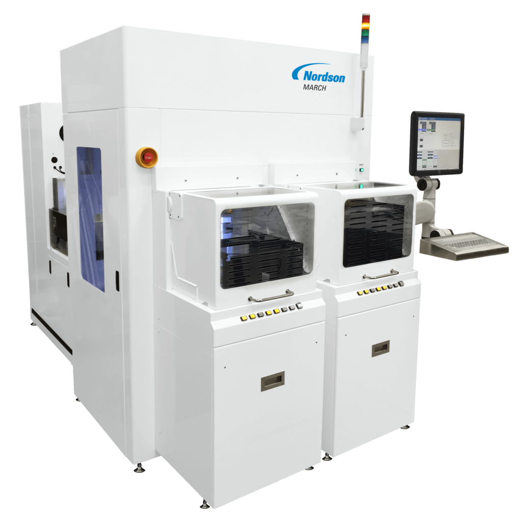
To address the challenge of handling these carriers and treating such thin wafers a variety of system configurations are available and are being developed. The SPHERE™ Series plasma treatment systems are capable of handling 300mm wafers, 300mm wafers on a supporting frame, and large panels for FOWLP/FOPLP. The StratoSPHERE™ system handles 200mm and 300mm wafers as well as 200mm wafers on a frame. For much larger wafers, the MesoSPHERE™ system has a larger chamber that handles thin 300mm wafers on a frame and larger panels up to 480mm x 480mm in size. Recently, our team of engineers developed a system with a much larger plasma chamber that can provide plasma treatment for panels as large as 650 x 650mm. The system is currently under evaluation at one of our customer sites.
No matter what the wafer size, the system should provide key plasma treatment performance requirements. The SPHERE systems provide a patented three-axis symmetrical plasma chamber to ensure that all areas of the wafer or panel are treated uniformly and provide exceptional etch uniformity and process repeatability, achieving >95% wafer-to-wafer uniformity and >90% within-wafer uniformity. Depending on the plasma recipe conditions, such as electrode configuration, power, and processing time, average etch rates with >3000 Å/min are achieved.
Tuning is another aspect of plasma control that must be considered, as it helps increase productivity and lower packaging costs. MARCH’s SMART Tune™ management system maintains performance through closed-loop plasma control that optimizes the RF system and minimizes tuning time.
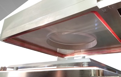
To maximize plasma control and effectiveness, a unique plasma confinement technology is incorporated in the plasma chamber. It uses a plasma confinement ring with the same diameter as the wafer to isolate plasma distribution directly above the wafer (Figure 3). The confinement ring turns a square plasma chamber into one configured for wafers. The ring concentrates and focuses the plasma directly over the wafer to speed up the etching process, provide uniform plasma coverage, and to isolate the plasma on the wafer itself rather than the area around or below it.

Using the confinement ring, there is a free conduction path between the upper and lower electrodes in the wafer region, but no conduction path in the adhesive tape, used to secure the wafer and the wafer frame area. The ring is not made of a carrier material, while the plasma conduction path is aluminum to aluminum only in the wafer area. Because there is no plasma generation or plasma to the bottom of the wafer and adhesive tape, undercutting and delaminating are minimized and there is no sputtering.
Process temperatures can be kept low because the ring increases etch rate capability without increasing the electrode temperature or adding bias to the chuck. An innovative handling system transfers round or square substrates and frame or bonded carriers. The modular design allows capacity increase on a per plasma chamber basis while equipment front end module (EFEM) integration supports from 1 to 4 plasma chambers.
Key applications for plasma treatment of fan-out wafer-level or panel level packages are:
- Cleaning of the substrate or panel surface to make sure it is contamination-free before the die attach process
- Surface preparation and activation in the pre-molding process to greatly improve mold adhesion
- The removal of sacrificial layer residues post wafer de-bonding
- Descum or removal of photoresist residues and pre-treatment to induce surface hydrophilicity for the Cu plating process
- The cleaning of metal pads and lines
- Treatment prior to die bumping to reduce organic and oxide contamination and improve adhesion of the bumps to the under-bump metallization (UBM) layer.
Larger wafers will be part of the semiconductor mix in the not-too-distant future, and with them, the need for plasma treatment of FOWLP and FOPLP packages. In the meantime, quality requirements are dictating the need for plasma treatment of all wafers in the advanced packaging process. It’s best to find a system that can meet today’s needs without compromising future requirements.
For more information, contact MARCH, Nordson Electronics Solutions, at info@nordsonmarch.com or visit the website at www.nordsdonmarch.com.