
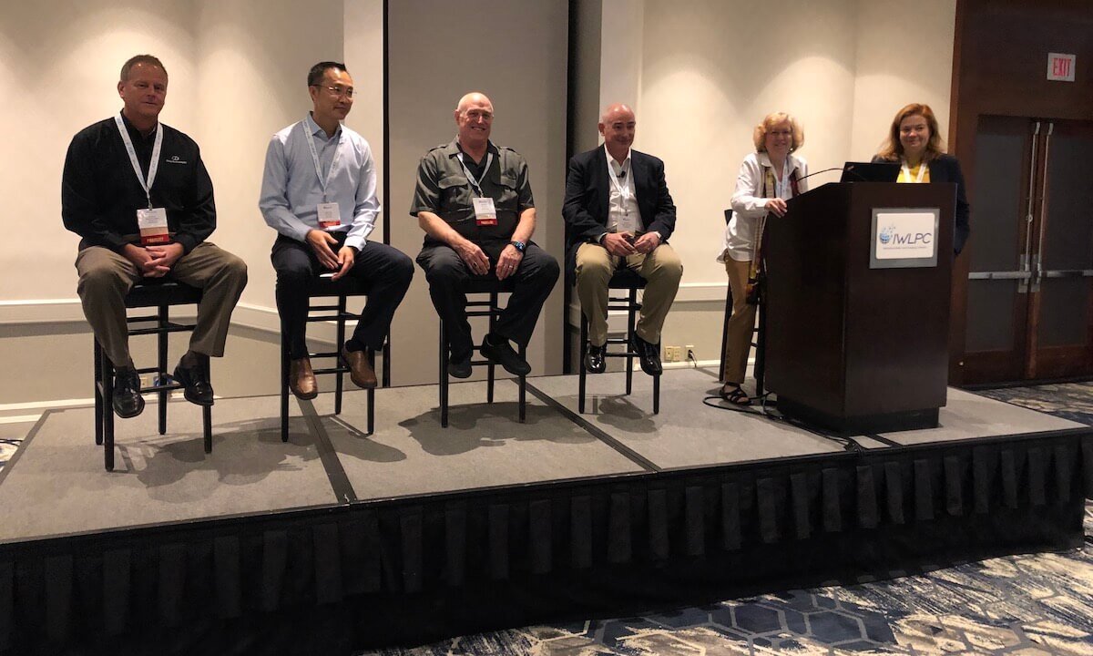
At IWLPC 2019, the fan-out panel-level packaging (PLP) debate continued in another of Jan Vardaman’s famous lively panel discussions, which was co-moderated by PLP technology expert, Tanja Braun, Fraunhofer IZM. Panelists were John Hunt, ASE; Joseph Dang, AT&S; Keith Best, Rudolph Technologies; Tim Olson, Deca Technologies.
Fan-out PLP (FO PLP) has been a hot topic on the conference circuit for a number of years, and we’ve been following its progress. According to JCET CTO, Choon Huang Lee, PLP may be the answer to yield and cost for emerging heterogeneous integration solutions like high-density fan-out (HDFO) and chiplet integration.
Deca’s Tim Olson says he’s been a believer in FO “before it was cool” and worked to bring innovation to it. Since the beginning, he’s worked to bring FO to large-panel format, and with ASE’s investment in 2016, it has helped bring it close to reality.
And while the volumes still aren’t high enough to ramp 600mm PLP into volume production, John Hunt says ASE’s 300mm chip-last PLP engineering line is ready to go, and the company’s 600mm M-Series line will be ready sometime in 2020.
On Fan-out PLP with 2µm l/s
Vardaman and Braun’s PLP panel discussion was intended to focus on meeting the challenges of achieving 2µm line/space requirements. And so the conversation started there.
Why do we need these finer geometries?
Keith Best, Rudolph, said it’s driven by 5G applications, to squeeze 2-3 more die into a package. Joseph Dang, AT&S, said cost is the driver, improving routeability on the fewest number of organic layers. He also said the PLP roadmap does include design rules down to 2µm l/s.
What are some challenges with achieving 2µm l/s?
There are a few, mostly related to lithography processes, and inspection. Automated optical inspection (AOI) equipment is limited at 2-3µm l/s. Copper migration isn’t an issue but may become one at 1µm l/s. Best said there may be a paradigm shift to damascene processes.
If we scale l/s will we also scale via sizes and capture pads?
Olson acknowledged this question, saying the most difficult part of scaling down is process work and equipment optimization.
In 2-3 years, which approach to FO will be leading to provide 2µm l/s, RDL first or mold first?
Hunt said there isn’t one right approach. They are implemented as needed in order of cost: The lowest cost is the chip-first eWLB, followed by the chip-first M-Series, and the then the slightly higher cost is the chip -ast fan out.
“We have all three capabilities,” he explained. “You can’t cram an application into a process. You have to tailor the process for applications.”
ASE has demonstrated 2µm l/s on 300mm round and can do it in production, noted Hunt. They are shooting for even finer features to create a higher productivity interposer replacement solution, such as for AMD’s Fuji products that combine two high bandwidth memory (HBM) chips with an ASIC and require sub-1µm l/s. “Cost is high, sourcing of interposers is challenging, and you can get better electrical performance using a hybrid FO solution,” he explained. He said 1µm l/s space has been demonstrated in engineering, but not in production.
What are the remaining challenges of PLP?
As it turns out, remaining PLP challenges have less to do with achieving 2µm l/s than working with panels themselves. Attendees were more interested in discussing things like substrate handling, materials deposition, and especially updates on standards surrounding panel sizes.

Dang, whose company, AT&S, manufacturers substrates in panel form, says that there are currently 6-8 substrate suppliers in the world who are manufacturing different panel sizes, and the lack of standardization is causing chaos because specific tools are required to handle different panel sizes. “We have to agree on a panel size because it impacts the equipment that we use to manufacture panels,” he said.
Long story short, 510 x 515 and 600 x 600 continue to duke it out, and it’s likely both will exist going forward. SEMI is working on FOUP standards to address both. ASE and Deca have adopted 600 x 600 as standard.
Hunt says using identical materials, such as spin-on photoresist for RDL patterning, is difficult, because you can’t spin material on panels. ASE uses slit die coaters instead and achieving uniform distribution hasn’t been an easy task. “We’ve demonstrated on low-density FO and must now take it to high-density,” he said. Additionally, handling and transport systems had to be designed differently to interface with panel tools. “You can’t manually lift the FOUPS, because they are very heavy,” he explained.
Best says after working for two years in a panel fab, Rudolph has solved most of the problems. “It’s easier than EUV,” he noted.
One of the biggest challenges in FO, in both round and square panels, is warpage, noted Olson. Some manufacturers opt for carriers, which are expensive and have limitations. He said Deca works to not use a carrier for 300 round or 600×600 square panels. This is a key consideration for equipment.
What about probe testing?
Here’s where 600 x 600 panels shine, because according to Olson and Hunt, the size was selected to ensure testability using existing probe testers. One 600mm panel segments into 4 300mm square, which is 15% larger than 300mm round. Probe manufacturers are already prepared to provide kits for existing probers to handle this. “There is better stepping efficiency, and tremendous test benefit,” noted Hunt.
What about meeting automotive reliability standards?
Here’s where Hunt clarified a couple things about FO in general for automotive applications, not just PLP. “Currently, the only wafer-level CSP in the infotainment system in the car, and the only fan-out in production for automotive is 77 Ghz (radar). These were selected for package size reduction and electrical performance improvement,” he explained. He explained that so far, automotive applications never needed FO packages, so nobody knows what they need to do to make FO meet automotive reliability standards. But, he cautioned, we will start seeing more automotive applications that will call for FO, such as networking systems, “so we’d better figure it out!” ~ FvT


