

It was in 1992 when Ted Tessier and I, in our paper, “Overview of MCM Technologies: MCM-D”, at the IMAPS Symposium in San Francisco, drew the analogy to the evolving LCD industry. “The LCD industry had spawned the development of a whole new class of large format, high-throughput thin-film processing equipment” and we proposed that these techniques could be applied or slightly modified to do high-density packaging like MCMs (what we today call system-in-package (SiPs). The IC industry was moving to larger and larger wafers, the LCD industry was moving to larger and larger panels so why not Advanced Packaging substrates? It seemed quite logical.
25 years ago, (1995) we sold DARPA on the logic of making high-density packages like MCMs on large-area panels (LAP). We put together a team of equipment vendors and tackled the problem on a 3-year, $25millon program entitled “Consortium for Intelligent Large Area Processing” or CILAP. This program was run from 1995 to 1998 by Dow Chemical and MicroModule Systems at their site in Cupertino CA.
The 1997 cover of IMAPS Advancing Microelectronics magazine (below) shows the LAP team. Some of you old-timers might recognize me without the beard, and Larry Moresco, in the upper right-hand corner. A section of the MMS clean room was set aside for the equipment to process our 400mm sq. panels. The panels were mainly glass (yes, we were using glass substrates 25 years ago) and anodized aluminum. Thinking ahead, we made sure that the material choices would be compatible with PWB for MCM-L.

Our equipment partners developed panel-sized coaters, exposure tools and plating tools (the size of the latter actually caused us to have to shut down the fab and knock out a wall to move the plating tool into the fab). Being a DARPA program, we didn’t have monies for automation and one of the unanticipated issues we ran up against was the fact that our wafer (panel) carriers which held 10 panels couldn’t be lifted or moved by the operators, so we needed a special electric cart to move them!
So, what happened to LAP in circa 1998? Basically, three years came and went and we never could get the yield up enough to move into production. Our goal was to produce 10-12um L/S (remember this was 25 years ago) and the tools just couldn’t meet spec to do that in acceptable yield. So we could make a lot of modules on a panel, but hardly any of them worked.
This is why when panel level processing burst into the scene again a few years ago, IFTLE has taken a wait-and-see attitude and continually pointed out that this new goal of 2um L/S on large laminate panels is not as easy as it looks on a PowerPoint slide. I think the old saying is “once bitten, twice shy” if you know what I mean.
3DInCites looked at the status of the exciting Fraunhofer /IZM Panel Level Processing Consortium in the summer of 2017. I think it is fair to say that in 2017 there was still a lot of work to do.
Now, more than two decades after CILAP, let’s take a look at where LAP (PLP) stands as of this year’s IEEE ECTC conference.
Cannon – i-line Stepper for Panel-Level Processing
A lithography challenge for fine-RDL in interposer applications is providing sufficient depth of focus (DoF) to accurately resolve sub-micron features. To meet this demand, Canon’s FPA-5520iV steppers can now provide new projection optics offering numerical aperture (NA) 0.24 imaging and 52 x34 mm exposure field. FPA-5520iV steppers with NA 0.24 provide 0.8 μm resolution performance throughout all imaging fields.
Warped wafer handling is a key challenge for BEOL exposure tools and the Cannon FPA-5520iV is equipped with a handling system that reportedly offers a significant improvement over first-generation FPA-5510iV steppers that were capable of handling up to 500 μm of wafer warpage. The latest FPA-5520iV steppers are designed to handle more than 5 mm of wafer warpage in order to process FOWLP reconstituted wafers that typically exhibit more warpage than silicon wafers.
Panel Handling
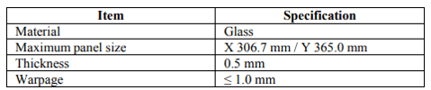
While maintaining 0.8 μm pattern fidelity across a large exposure area is a key requirement of fine RDL processes, Fanout (FO) technologists seek to transition from wafer-based to-panel based processes to improve productivity and costs. To support high-resolution FOPLP processes, Canon is studying a panel handling system for FPA-5520iV steppers. Although FPA-5520iV steppers cannot yet process 730 x 920 mm panels (Gen 4.5 ) they have developed a substrate handling system for R&D purpose which handles 365 x 306.7 mm panels ( 1/6 of a Gen 4.5 panel) providing 0.8 μm resolution. Details of the allowable substrate range for the FPA5520iV panel handling system are included in the table below.
Semsysco GmbH – Panel-Level Plating
Semsysco GmbH discussed panel level processing in their paper “Advances in high-speed plating for vertical glass panel fine-line plating”. The main hurdle to provide 2um L/S is that the panel typically has to be handled vertically, and cannot be rotated to achieve optimal uniformity, which can drive the costs up, as more time is required to deposit overburdened films that must subsequently be polished and etched. To overcome this issue, they report their plating solution replenishment is so close to the substrate surface, that they claim to effectively minimize the surface boundary layer such that the exchange of the electrolyte occurs effortlessly. High plating speeds, require large electrical fields to drive the currents, and this electric field impedes the chloride ion from reaching the cathode. Their system overcomes this by direct injection close to the surface and therefore improves the plating speed of all electrolytes. They report that the system scales with substrate sizes of 510 x 515mm², 600 x 610mm², 620 x 750mm² (GEN 3.5). They report blanket uniformities around 2%, and patterned substrate uniformities of 5-7%.

IME / A STAR – Panel-Level Warpage
IME / A STAR discussed their modeling presentation “Study on Warpage of Fan-Out Panel Level Packaging (FO-PLP) using Gen-3 Panel” where FEA was used to investigate warpage during panel level processing on a Gen-3 glass substrate (550mm × 650mm size). Material selection and structural design were considered. The effect of gravity on the panel warpage was simulated and analyzed. Modeling gravity effect reduces the panel warpage significantly, making results closer to the real case.
In this study, the package size is designed as 15mm × 15mm with embedding single chip with a size of 10mm sq. Packages are fully populated in Gen 3 panel with an array of 34 rows by 40 columns, so there is a total of 1360 packages in one panel. The figure below shows the IME / A Star process flow for FO-PLP packaging technology. A very thin laser release layer, used for the debonding process, is coated onto a glass panel carrier. Then, dielectric coating, lithographical patterning, seed layer deposition, photoresist coating, and development are conducted for preparing the RDL layer plating process. Two RDL layers are fabricated on a glass carrier panel by repeating the above processes. Then chips are bonded to panel with Cu pillar connections.
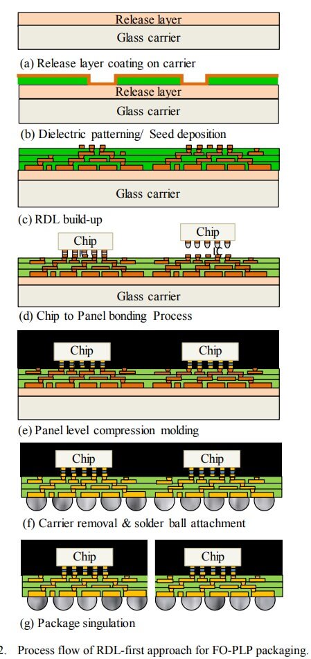
After that, panel-level compression molding using an epoxy molding compound (EMC). Either liquid or granule EMC can be used for the compression molding. According to the designed package thickness, the back grinding process of the EMC layer is carried out. After panel back grinding, the glass carrier is removed through a laser debonding process. Next, the solder ball attachment process can be carried out on the partitioned panel. Finally, a separate package can be achieved after the singulation process.
Based on FEA simulation results and experimental correlation of panel warpage for FO-PLP technology, they concluded:
- Using thick glass carriers helps to reduce the panel warpage significantly for the RDL process.
- Glass carrier should have matched CTE with EMC material to reduce the panel warpage after the molding process.
- Chip and over-mold thicknesses, dielectric and EMC materials are important parameters affecting the panel warpage after debonding.
- Gravity helps to significantly reduce panel warpage of the thin large panel.
Based on optimized structure and materials, the panel warpage can be controlled less than 7mm in each process step for 550mm × 650mm panel.
BESI – Pick-and-Place for Panel-Level Processing
Besi experts discussed “Large Panel Size Bonder with High Performance and High Accuracy”. This paper presents a panel-level die-attach machine suitable for substrates up to 730 mm x 920 mm (GEN 4.5). The bonder provides global placement accuracy of 2 μm @ 3σ and local placement accuracy of 1 μm @ 3σ at 6000 UPH, the bonder’s productivity can be scaled up to 7000 UPH. The equipment can be configured for various fan-out pick and place processes, for silicon bridge embedding, thermal compression, and other processes.
Although PLP on the roadmap of nearly every outsourced semiconductor assembly and test (OSAT) company there is yet no standardization in panel size. Current sizes vary between 510 x 415 mm² (SEMCO), 510 x 515 mm² (Intel), 600 x 600 mm² (ASE/ DECA) and in some cases even up to 730 x 920 mm² (GEN 4.5).
Besi’s PLP Die Bonder reportedly supports panels up to 730 x 920 mm². A die-attach cell with a dual gantry pick & place system can be linked with a broad variety of process modules including:
- flip-/non-flip module
- heated bond head and heated panel chuck
- Thermo compression bond head
- multi-die handling with auto tool exchange
- thin die ejector (> 50μm die thickness)
- multi-nozzle bond head and die provider to support enhanced accuracy at the sub-micron level on panel
Conclusions:
The industry probably won’t move right into high-density production [ 2/2] so when you see statements that some OSATS “already” have their PLP lines in place be sure to search the detail in terms of whether we are really talking 2/2 L/S and <5um high-density vias and whether all the unit ops are being run on panel sized equipment.
We have certainly come far since 1995, but IFTLE still does not see ALL of the equipment in place YET…
For all the latest on Advanced Packaging stay linked to IFTLE……………………


