

![]() Fan-out wafer-level packaging (FOWLP) is an emerging type of high-density advanced packaging (HDAP) technology in the semiconductor industry that is rapidly gaining popularity in the market. But what exactly is FOWLP? Why do we need it? How do we take advantage of it? What limitations still need to be overcome?
Fan-out wafer-level packaging (FOWLP) is an emerging type of high-density advanced packaging (HDAP) technology in the semiconductor industry that is rapidly gaining popularity in the market. But what exactly is FOWLP? Why do we need it? How do we take advantage of it? What limitations still need to be overcome?
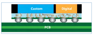
FOWLP brings single and multi-die designs together, combining multiple die from heterogeneous processes into a compact package (Figure 1). The die are embedded in an epoxy mold compound (EMC), then die-to-die and die-to-ball-grid-array (BGA) connectivity are established directly through the package redistribution layer (RDL), without the need for through-silicon vias (TSVs) or a laminate package substrate. While FOWLP typically requires a silicon wafer as a carrier, this wafer does not remain in the package. Eliminating TSVs and the substrate not only reduces production costs, but also enables companies to make very thin packages, which provides electrical advantages.
FOWLP designs also provide the option of placing even more components vertically, using through-package vias (TPVs) that allow for package-on-package (POP) design. Unlike TSVs, TPVs act much more like the traditional package vias, reducing concerns about yields and reliability. TPVs are also less sensitive to inductive and heating effects than TSVs, as well as being less expensive to produce. The PoP design provides a smaller footprint, which enables designers to stay within vertical requirements, and allows a wide choice of 3rd party DRAM in the package. With their promise of smaller form factors providing low power with high performance [1], it’s easy to understand the growing popularity of FOWLP. Smartphones and wireless multimedia are the first large commercial segment to use FOWLP designs, as seen in the newest iPhones from Apple.


