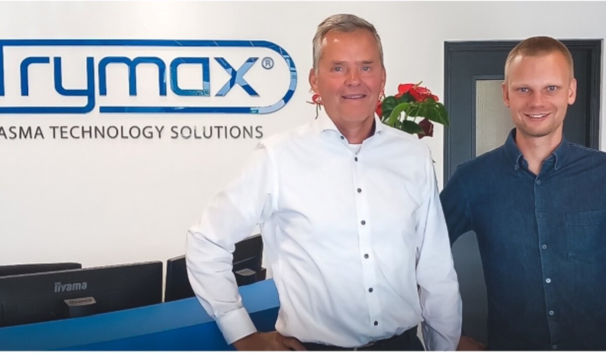
This interview with Trymax Semiconductor’s Peter Dijkstra, Chief Commercial Officer (CCO), and Karsten Arts, Process Engineer first appeared in Atomic Limits as part of a series of posts about companies within the atomic scale processing industry. The goal of the series was to provide information about the kind of products and projects the companies have and how they see their company developing in the future. They also discuss how the companies implement science communication and which student opportunities exist.
Trymax’s core mission is supporting global semiconductor manufacturers with its innovative plasma-based equipment solutions. Photoresist stripping, a critical step in the semiconductor manufacturing process that involves the adequate removal of the photoresist layer from a wafer is the company’s primary process. With its innovative solutions, Trymax aims to meet the most stringent requirements and deliver advanced processing capabilities to push the boundaries of the semiconductor industry.’
The History of Trymax
Leo Meijer, the CEO and founder of Trymax, started his career in the semiconductor industry at Philips Semiconductors (now NXP). Here he became responsible for overseeing a group of maintenance engineers at the Philips factory in Nijmegen. After some years, he transferred to Matrix Integrated Systems, a chip machine manufacturer based in the United States to take on the role of senior field service engineer.
However, in 2003, the landscape shifted when Axcelis Technologies acquired Matrix. Axcelis, primarily interested in the latest chip machine models, made the decision to discontinue support for its European customers. This left a significant void in the market and posed a challenge for the large customer base in Europe that relied on Matrix machines. Recognizing the opportunity to fill this gap, Leo reached out to the European customer base to continue providing valuable service and maintenance and was soon joined by Ludo Vandenberk (Executive Vice President) whom Leo knew from his time at Philips and Matrix.
In 2003, Trymax, an anagram of “Matrix”, was founded on the clear mission to provide service and support for European customers who depended on Matrix machines. As time went on, however, Trymax faced a new challenge. Between 2009 and 2011, it became clear that the aging Matrix machines had exceeded their serviceability limits. So Trymax began manufacturing its own machines.
The company underwent a significant transformation, transitioning from a service-oriented company to a cutting-edge manufacturer. This strategic move allowed them to adapt to the evolving semiconductor landscape and stay at the forefront of technological advancements.
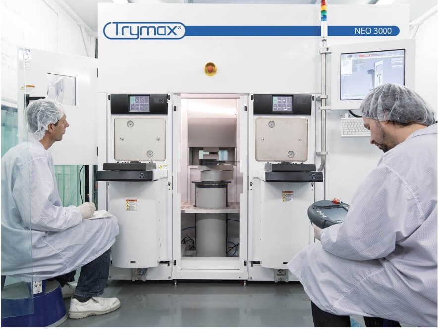
During this period, Trymax introduced its proprietary product line known as “NEO,” designed to address a wide range of applications throughout the semiconductor manufacturing process. The name “NEO” pays homage to the main character of the iconic 1999 movie “The Matrix,” of which both Leo and Ludo are fans. (Figure 1)
What are Trymax’s target process applications?
The primary focus of Trymax is photoresist stripping, which is a crucial step in semiconductor manufacturing that involves the adequate removal of photoresist material from a wafer after the etching step. They use remote microwave plasmas at substrate temperatures around 250 °C to “burn off” the photoresist in a process called ashing. In a remote plasma, O2 is dissociated, and an abundance of radicals is produced that are channeled to the wafer. Alternatively, the plasma can be generated in an RF parallel plate reactor at lower temperatures, generating more ions. Trymax also works on machines that combine microwave plasma generation and an RF-powered wafer chuck.
Trymax tools are also used to “descum” wafers, which removes residual photoresist (scum) left in the open features of the pattern after the lithography and developing steps. This process takes place at lower temperatures to prevent damage to the patterned photoresist. Here, the challenge lies in delicately removing a small amount of photoresist while preserving the integrity of the pattern.
UV curing solutions are also part of Trymax’s offering. A UV source used during the photoresist baking step forms a crosslinked “crust” as a top layer. This helps prevent reflowing, which leads to pattern loss. UV curing also helps with the future removal of resist. Without UV curing, the photoresist can start cooking during the ashing step. This leads to photoresist “popping”, during which unwanted particles contaminate the wafer.
Looking ahead, Trymax is following the development of Industry 4.0. This next-generation system aims to establish seamless communication between machines throughout the production chain. By optimizing process matching and minimizing downtime, this system allows machines to autonomously take over in the event of malfunctions. While operators currently oversee these operations, the future integration of artificial intelligence holds great promise.
What makes Trymax unique?
Trymax has three main areas of expertise: low-temperature plasmas, wafer transport, and material processing. Regarding wafer transport, Trymax supports exotic materials like silicon carbide and gallium nitride, and unique structures, like TAIKO wafers. These wafers come in different sizes and thicknesses.
TAIKO wafers are ground down to 30µm in the active area, leaving an outer ring that is kept at the original thickness of 735µm for support. These extremely thin wafers require delicate handling (Figure 2).
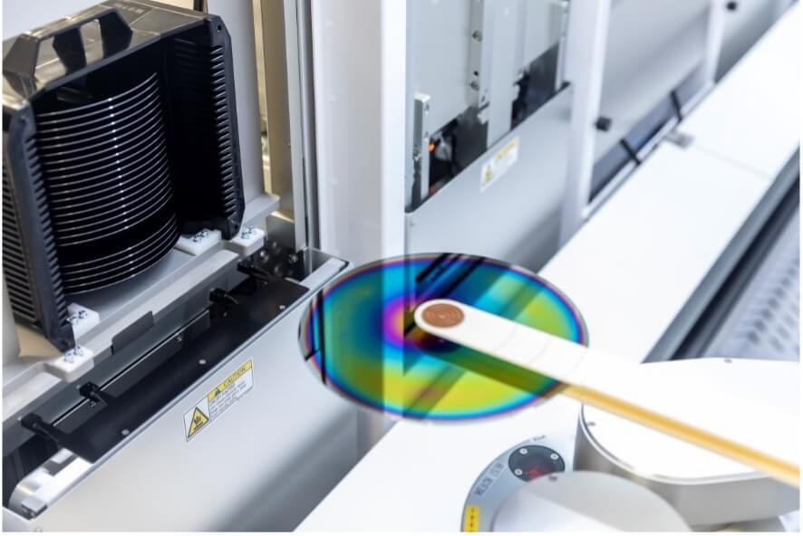
To accomplish this, Trymax uses a sophisticated robot arm equipped with specialized substrate gripping solutions, designed for a wide range of conditions. To ensure clean wafer transport, the company’s 200mm wafer tools are equipped with Standard Mechanical Interface (SMIF) technology. Its 300 mm processing tools utilize Front Opening Unified Pod (FOUP) technology for transport. To adapt to the evolving market, Trymax is currently in the process of rebuilding its systems to support overhead transport. This modification automizes wafer cassette loading from the top, allowing for a more efficient operation.

A notable feature of Trymax’s equipment is its ability to process two different wafer sizes simultaneously. This proves particularly valuable in a transitioning market, such as the LED industry (going from 150 to 200mm), where older machines need extensive modifications to accommodate new wafer diameters. By already accommodating varying wafer sizes, Trymax’s machines mitigate the risks associated with equipment reconfiguration. An additional feature is that the machines automatically recognize the wafer size and handle it seamlessly, streamlining production processes and enhancing efficiency.
Lastly, Trymax employs a talented team of experts in the field of low-temperature plasmas leading to innovative plasma sources and solutions. While the company primarily focuses on applied research, in the future, it would like to collaborate with universities to engage in more fundamental research. One approach to foster this collaboration involves granting universities access to one of their machines, enabling them to conduct research and explore new possibilities in plasma processing.
Who are Trymax’s target customers?
Targeting a diverse range of markets, Trymax focuses on delivering innovative solutions to cater to the specific needs of various industries. The company primarily serves three main markets: the automotive industry, cloud computing, and 5G technology.
In the automotive sector, Trymax products help in power-related applications, specifically in the current transition to electric vehicles. For these power electronics devices, ordinary silicon is not an option as it cannot withstand high voltages. Trymax provides a solution by being able to process gallium nitride (GaN) and silicon carbide (SiC) wafers, which are suitable for power electronics. Similarly, for 5G, Trymax provides a solution of processing wafers other than silicon, needed for this advanced technology.
Cloud computing is a technology that enables the delivery of computing over the internet. It provides on-demand access to resources such as storage, processing power, and applications, without the need for local infrastructure. However, to meet the ever-rising processing speed requirements at the cloud stations, more optical fibers are being implemented. Trymax’s products come into play by facilitating the manufacturing of IR lasers used for signaling over these fibers.
In addition to these primary markets, Trymax recognizes the growing significance of other sectors such as biomedical, artificial intelligence (AI), and the Internet of Things (IoT).
In terms of market presence, the primary market is Europe, with a particular focus on automotive applications originating in Germany. The second largest market is China whereas other significant markets include Southeast Asia, the USA, Taiwan, and Japan.
Does Trymax actively pay attention to science communication?
Like any other company, safeguarding its intellectual property and proprietary findings is important to Trymax. However, it recognizes the significance of communication. Therefore, Trymax actively seeks opportunities to engage with clients and the wider scientific community. They often participate in events and conferences to showcase their expertise, network with industry professionals, and stay current on the latest advancements in the semiconductor industry. Trymax is launching a newsletter specifically designed for its clients, serving as a platform for sharing updates, technological breakthroughs, and other relevant information directly with its client base.
Looking ahead, Trymax acknowledges the potential benefits of collaborating with technical universities. By partnering with them, the company seeks to establish a stronger presence in the scientific community. Linking the Trymax name to research publications will enhance its reputation and visibility in the industry. However, as the company is growing at a fast pace, finding the time to work on these papers can be an issue. Nonetheless, Trymax is full of ideas that they are eager to explore and develop further.
About the Trymax Team
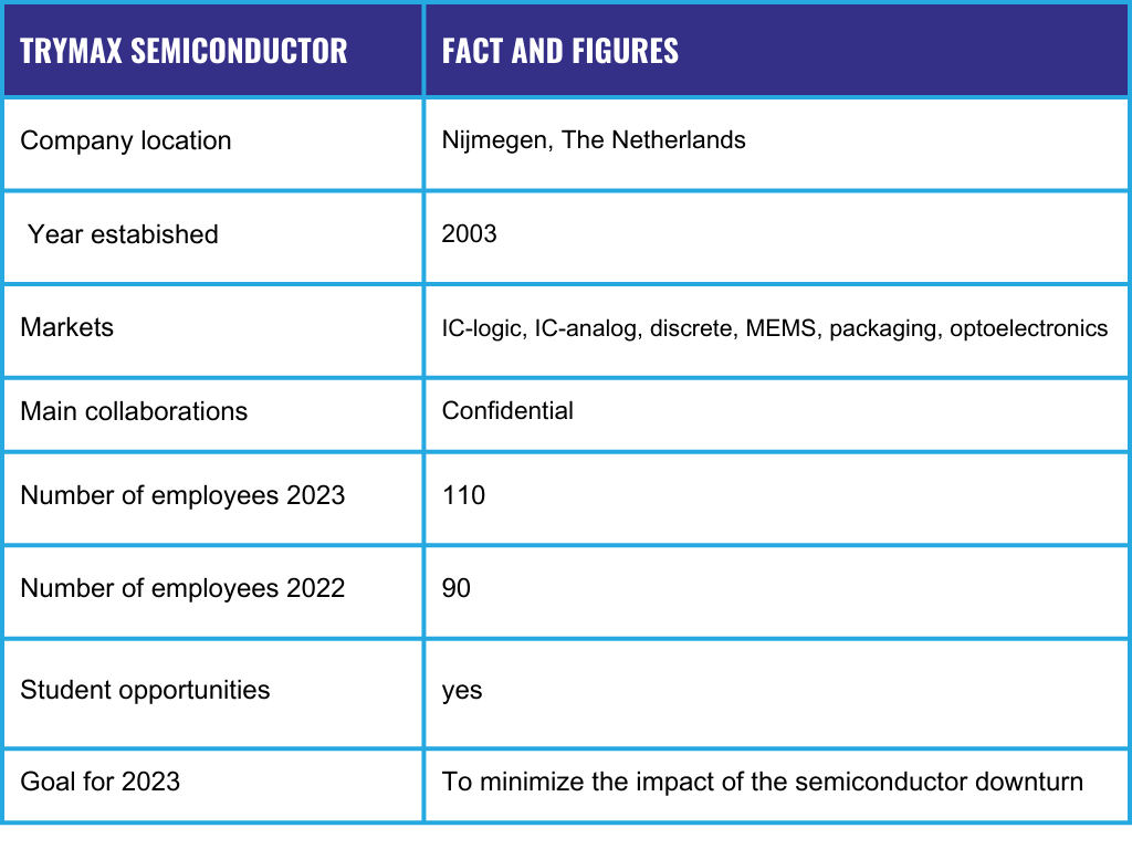
Trymax is experiencing significant growth and comprises diverse professionals with a range of expertise. Over the past year, Trymax has expanded its workforce from 90 employees in 2022 to 110 employees in 2023, indicating the company’s positive trajectory and increasing demand for its services.
A notable characteristic of the team is the presence of many young and innovative engineers. These fresh-minded individuals bring a dynamic perspective to the company, contributing to its innovative culture. They hail from different backgrounds, including applied physics (especially in process engineering), mechanical engineering, and electrical engineering, bringing a multidisciplinary approach to problem-solving and product development.
Recognizing the value of young talent, Trymax offers internship opportunities for students. While they only had one physics-related internship thus far, the company is happy to welcome new students. By providing internships, Trymax not only contributes to the development of future professionals but also benefits from the fresh ideas and perspectives brought by the interns.