
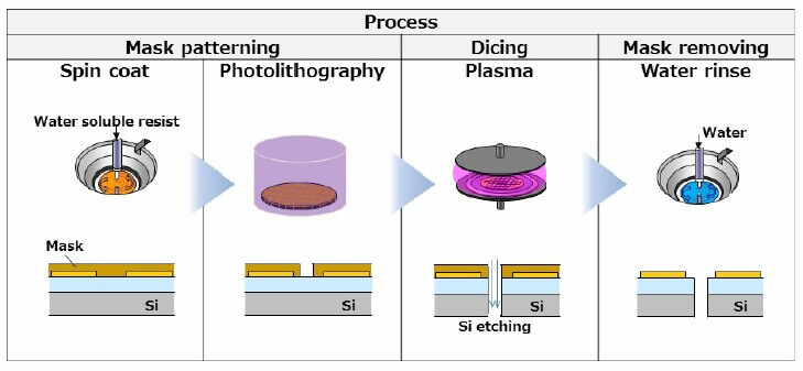
Plasma Dicing
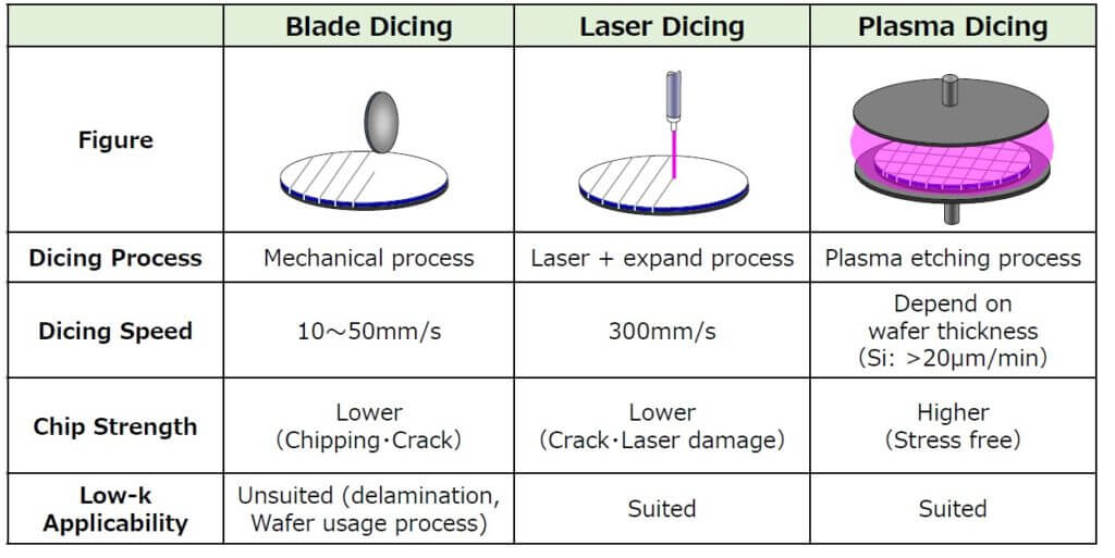
Advanced packaging is bringing with it new ways to separate die from the wafer. In the past, wafer dicing was traditionally carried out using conventional dicing “saw”. However, this method has limitations such as die chipping or cracking leading to lower device yields. Also, the width of the blade removes valuable “real estate” from the wafer. Newer techniques include laser and plasma techniques. These are compared in Figure 1. More information can be found here.
Dry plasma can be used etch very narrow trenches into silicon to separate individual die. Advantages of plasma dicing include:
- All dicing streets are etched simultaneously, resulting in greater throughput
- plasma dicing will not damage the wafer surface or affect trench sidewall, which can result in greater die strength, improved device reliability and increased device lifetime
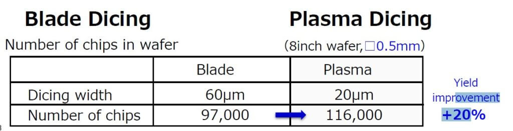
- The narrower street widths of plasma dicing allow for increased die count per wafer
- Non-rectangular die shapes can also be created (i.e. defined by mask, not blade cut)
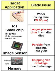
Panasonic indicates that they are focusing on applications such as small die, image sensors and memory as seen in Figure 3.
EV Group and Panasonic have recently announced that they have developed a novel resist processing solution for plasma dicing applications, such as IoT sensors, MEMS, RFID, CMOS image sensors and thinned memories. This solution incorporates the EVG®100 series resist processing system and Panasonic’s APX300 Dicer Module plasma dicer (Figure 4).
Plasma dicing enables highly parallel and high-throughput die singulation for small devices such as sensors, MEMS and RFID chips. It also provides debris- and particle-free die singulation to enable high process yields for CMOS image sensors, as well as damage-free and high-quality chip sidewalls for thinned memories.
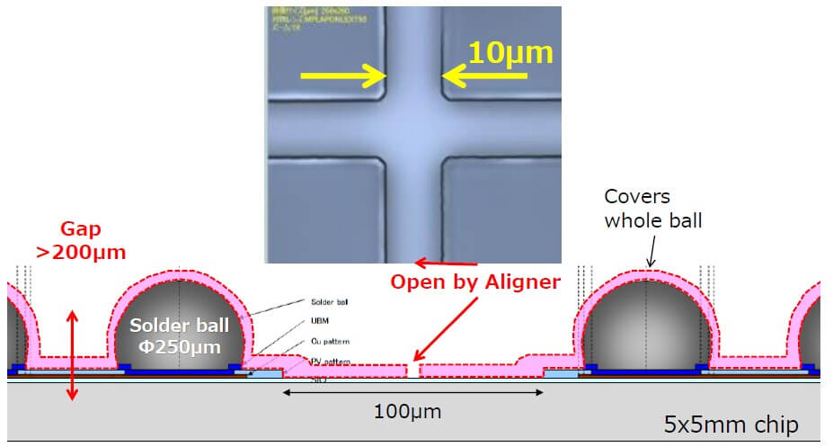
Plasma dicing brings new pre-process requirements, including the need for thick resist coating (several dozen microns thick) on the wafer’s surface prior to lithography or laser patterning processes to open up the dicing lanes. However, uniform protective coating of structures on the surface, such as multi-layer interconnections and bumps, is critical with traditional spin-coating techniques (Figure 5).
Intel
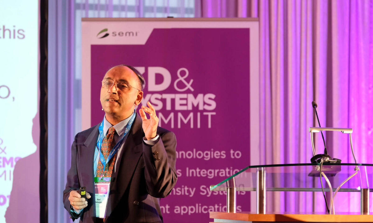
At the recent SEMI 3D & Systems Summit, Ravi Mahajan of Intel presented an interesting perspective on heterogeneous integration (HI) and 3D packaging entitled, Advanced Packaging: A Perspective on 2D and 3D Packaging”. HI of disparate compute and communication functions is a key enabler of performance in today’s microelectronic systems. HI refers to the integration of separately manufactured components into a higher level assembly (SiP) that provides enhanced functionality and improved operating characteristics.

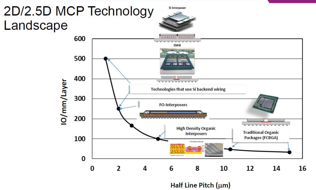
High bandwidth demand has spurred recent interest in such dense multichip packages. Technologies with silicon back end wiring provide the highest wiring densities as shown in Figure 6.
Mahajan compared the pros and cons of Intel’s EMIB and Si Interposer technology as shown in Figure 7.


Mahajan contends that the future requirements for multichip packages will be 1000s of IO /mm with greater than a Tb /sec bandwidth using bump pitches of 10µm as shown below. It will be interesting to see exactly where Intel ends up deploying these two technologies.
For all the latest in Advanced Packaging stay linked to IFTLE….


