
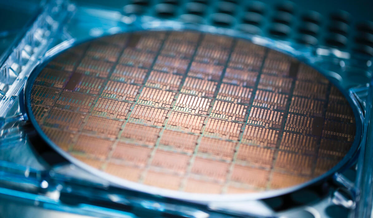
CEA-Leti and Intel recently announced a new collaboration effort on advanced 3D packaging technologies for processors to advance chip design. The research focuses on the assembly of smaller chiplets optimizing the interconnect technologies between the different microprocessors and on new bonding and stacking technologies for 3D ICs focused on high-performance computing (HPC) applications.
Hardly a week goes by without an announcement on artificial intelligence and the need for improved HPC to analyze the data closer to where the data is collected. Intel has been releasing new developments, creating new systems that instead of being a single piece of silicon normally called a system on chip (SoC), which has been used in the past, for computing processing units (CPU) in data centers.
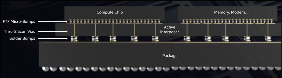
Intel is now developing three-dimensional (3D) technologies such as EMIB and Foveros (Figure 1) to combine different high-performance chips such as a CPU, GPU, neural network chips, and memory into the same package or system. These new combinations have been defined as heterogeneous compute, and the techniques to combine them heterogeneous integration. The advantage of these systems is that they provide better analysis of the data in a shorter period of time, at hopefully lower power consumption.
CEA-Leti and Intel have had a long relationship developing compute technology. The last agreement enacted in 2016 was focused on developing technology to facilitate the internet of things (IoT). The new collaborative agreement, while not specifically focused on IoT, deals with the efforts to develop new HPC technology that will be used to analyze and react to the data created by the digitization of businesses formerly known as the IoT.
CEA-Leti brings to the deal its strength in 3D silicon research, including work on the ‘IntAct’ demonstration, a silicon active interposer as a promising solution towards 3D heterogeneous integration, which won the best paper award at the June 2019 IEEE Electronic Components and Technology Conference. Intel brings its strengths in developing and manufacturing silicon for HPC, along with the recent work in the Foveros packaging technology.
The quest for integration of different chips onto the same platform has been taking place for some time.
When through-silicon vias (TSV) were introduced, the industry was hopeful that stacking chips with different functions was just around the corner implementation of direct chip-to-chip integration was hindered by the heat generated from the CPU which was difficult to remove from the closely packaged chips. Many years later, this quest is finally starting to bear fruit with multiple processors, or chiplets, stacked onto an interposer for better compute performance.

In a discussion with Severine Cheramy, 3D business development director at CEA-Leti and Director of the 3D program of IRT Nanoelec, she explained that there are multiple challenges in stacking multiple HPC chips in the same package. Heat, test, bonding devices together, and shrinking the pitch of the bumping to be able to effectively shrink the size of the final package are just a few. The combined work will look at how to better bond the chips together. This could mean redesigning the upper layers of interconnect in HPC and memory chips to enable the shrinking chip-to-chip connections. Cheramy said that the R&D will take place in Grenoble, France at the CEA-Leti facility.
From an advanced 3D packaging perspective, the collaboration combines two 3D powerhouses, and based upon the long-standing working relationship it is a good combination for advanced chip development for HPC.


