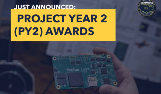
The Microelectronics Commons NSTXL (National Security Technology Accelerator) has announced the DoW Year 2 awards, with more than $200M invested across 26 projects nationwide and the Southwest Advanced Prototyping (SWAP) Hub earning continued support for multiple high-impact efforts already advancing U.S. microelectronics innovation. These awards recognize real progress and growing...
Why copper grain size matters for hybrid bonding and how to control it for HBM and chiplets. Read the article here. Abstract Hybrid bonding is reshaping advanced packaging by enabling ultra-fine pitch copper-to-copper interconnects, essential for high-bandwidth memory (HBM), chiplet integration, and 3D heterogeneous systems. While alignment precision, oxide control,...
A patient who can no longer speak generates text directly from neural activity. A patient with paralysis controls a cursor using thought alone. Behind demonstrations like these is a difficult engineering problem: how do you assemble electronics delicate enough to interact with the human brain, while keeping them stable inside...
By Thomas McMahon Naval Surface Warfare Center, Port Hueneme Division, CA Sailors can now get certified in operating and maintaining the fleet’s most prevalent directed energy system through a new training program at Naval Surface Warfare Center, Port Hueneme Division (NSWC PHD)’s Directed Energy Systems Integration Laboratory (DESIL), with the first...
Advanced packaging has continued to evolve with various interconnect technologies on their way towards heterogeneous integration. Different assembly processes are...
Understanding the role of compromises and trade-offs in the design process Electronic packages serve many purposes including protecting, connecting, and...
Artificial intelligence and machine learning (AI/ML) can have various applications in smart manufacturing for semiconductor fab, advanced packaging, and electronics...
Electronics Packaging vs. Advanced Packaging Electronics packaging is generally divided into three major areas, traditional packaging – also called standard...
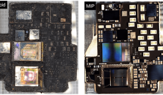
Determining the causes of failures in semiconductors often requires removing overlying material to expose the failed circuit element for high-resolution...
Economics are forcing semiconductor manufacturers away from traditional 3D through silicon via (TSV) packaging integration. The future of advanced packaging...