
Determining the causes of failures in semiconductors often requires removing overlying material to expose the failed circuit element for high-resolution imaging in an electron microscope (EM). Bulk techniques, such as mechanical cutting and polishing, can create additional defects due to induced mechanical stresses, and, like broad ion beam milling, they lack the required site-specificity. Focused ion beam (FIB) can be used to expose specific sites, but it is quite slow for larger spatial dimension tasks.
Combining laser ablation, to remove the bulk of the material, with FIB, to cut and polish a final cross-section of the suspect element, achieves the speed and precision needed in this operation. The latest iteration of this combined approach, which implements parallel processing with laser ablation and Plasma FIB, provides additional increases in analytical throughput, efficiency, and flexibility.
FIB systems are widely used to cross-section circuit elements for subsequent imaging and analysis in an electron microscope or other analytical tools. The nanometer-scale precision with which the FIB cutting action can be controlled permits the operator to accurately dissect even the smallest features of the circuit. However, this precision comes at a cost. FIB milling rates are quite low, especially with gallium (Ga) FIBs, making their use to remove large volumes of overlying material prohibitively slow and costly.
A decade ago, the introduction of plasma sources (Plasma FIB), which permit substantially higher beam currents than conventional liquid Ga sources, increased FIB milling rates with an acceptable trade-off in milling precision. However, over that same period, the failure analysis challenge also increased as device manufacturers developed advanced heterogeneous integration and packaging techniques that combine multiple ICs in a single package. The feature of interest in these packages may be buried below several layers of circuitry or multiple dies. The volume of overburden that must be removed to reach specific circuit elements has grown tremendously, from cubic micrometers to cubic millimeters, while the elements themselves have continued to shrink.
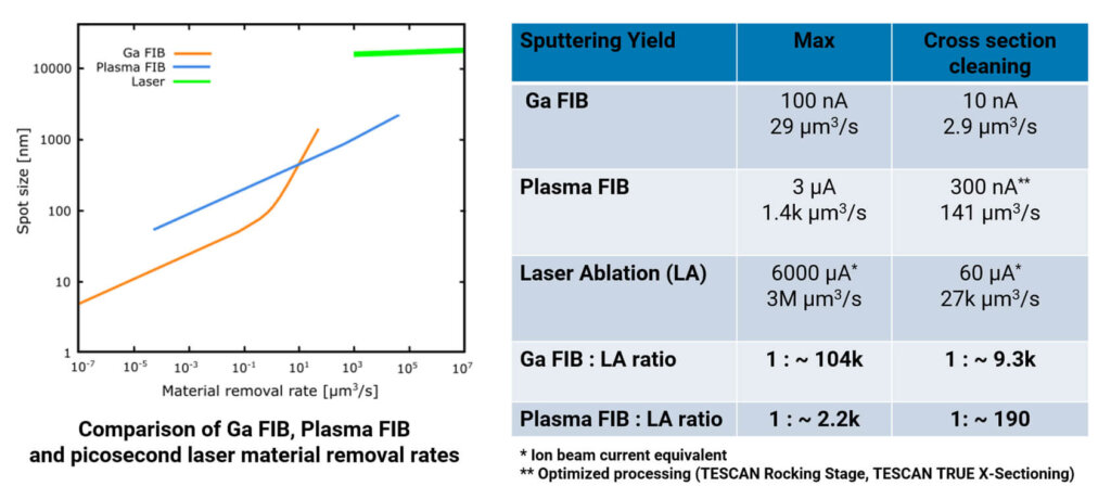
Laser ablation offers maximum milling rates that may be 100,000 times faster than Ga FIB and 2,000 times faster than Plasma FIB, while still retaining sufficient milling precision to target specific features. Combining laser ablation, for bulk material removal, with Plasma FIB, for final cut and polish, can reduce the total time needed to prepare a deep cross-section as much as 95%, or more for specific cases. Figure 1 shows the relation between spot size and material removal rate for Ga FIB, Plasma FIB, and laser ablation. The adjacent table provides a numeric comparison of material removal rates for the 3 techniques at maximum milling and final polishing beam conditions.
The first systems to integrate laser ablation with FIB did so by incorporating the laser within the FIB chamber. In this configuration, the system can use only one capability at a time, leaving the other function idle. A new approach implements the integration strategy using correlative microscopy techniques to provide parallel processing through stand-alone laser ablation (microPrep PRO, 3D-Micromac AG) and Plasma FIB (TESCAN Solaris X) systems. Neither system is idled by the operation of the other. The laser ablation system can prepare samples for multiple downstream tools, whether they be multiple FIBs or various other failure analysis tools. The net result is an increase in analytical throughput and productivity that ultimately reduces the cost per analysis.
The laser ablation system provides milling precision/spot size of about 10 micrometers and beam placement precision of about 3 micrometers over centimeter distances, allowing it to remove cubic millimeters of material quickly and accurately. Correlative alignment techniques based on overlays of CAD data from the circuit design or 2D images from various previous FA tools facilitate finding the feature of interest with high precision in both systems. Parallel processing in stand-alone systems offers several benefits. Ultrashort laser pulses minimize the so-called heat-affected zone and thus the amount of material that must be removed by final polishing in the Plasma FIB. Removing bulk material in the laser ablation system avoids the risk of excessive contamination of the Plasma FIB where contaminants can interfere with the tool itself and analytical results as well. The sample can be processed by the laser in a variety of gas environments, and solutions are available to permit transfer between systems without exposure to the ambient environment. The stage on the laser ablation tool provides precisely automated movement with six degrees of freedom, allowing it to mill complex patterns when needed. The ability to tilt the sample during the laser ablation process is especially beneficial to compensate for taper caused by the Gaussian intensity profile of the beam. Although taper can be eliminated in final polishing with the FIB, avoiding its creation during the laser ablation operation can greatly reduce the time needed for final FIB clean-up. Eliminating taper is critical in precisely aligning the cross-section through stacked repetitive structures in the semiconductor samples (e.g., TSVs, micro bumps).
The Plasma FIB system is optimized for deep, large-volume milling. It offers beam currents up to 3 µA, which can remove up to 1,400 µm3 of material per second. Lower beam currents (300nA) used for final cleaning and polishing still remove up to 141 µm3/s and deliver pristine cross sections even on challenging samples. The most challenging samples are those that combine hard and soft materials that mill at very different rates. The harder materials mill more slowly and tend to shield the regions below, creating distinctive vertical artifacts descriptively called “curtaining”. Curtaining can be especially troublesome in composite materials where harder fibers or particles are dispersed in a softer matrix – metal interconnects, Si, and dielectrics in semiconductor samples. Curtaining artifacts can obscure critical details in subsequent imaging. They can be reduced by rocking the sample repeatedly through a small angle during the milling operation. The slight changes in angle give the beam better access to the shielded regions below the harder materials and smooth out the milling process. Curtaining can be a challenge for FIBs at higher beam currents/milling rates, like those needed for high-speed milling in a large volume workflow. The Rocking Stage of the Plasma FIB system used for this work provides an automatic rocking mode.
Terracing is another artifact induced in certain materials, including silicon carbide, polyimide, glass, etc. It results from the dependence of the material removal rate on the incident angle of the ion beam. Removal rates are generally highest at grazing incidence, as at the face of the cross-section, and lowest at normal incidence. For this reason, terracing, once it appears, is self-reinforcing and can be very difficult to remove. Terracing can be avoided by creating a hard mask on the surface of the sample before milling. The mask can be deposited in the FIB using the beam to decompose specially chosen precursor gases injected near the beam and sample surface, but the deposition process is slow and not amenable to a high-volume workflow where the overriding consideration is speed. An innovative solution (True X-Sectioning, user-guided procedure) allows the operator to place a small protective hard-mask over the area to be sectioned. This procedure eliminates terracing artifacts and is significantly faster than large area FIB deposition.
Examples
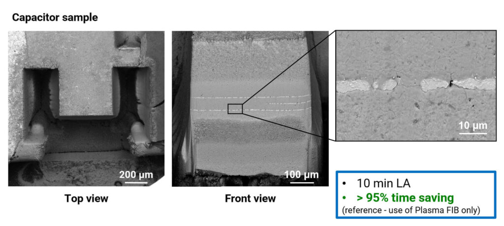
Figures 2 through 6 show examples of the use of laser ablation and Plasma FIB to expose circuit elements for imaging and analysis. Each example includes the time spent in each operation and the total time saved relative to preparing the sample with Plasma FIB alone.
Advanced Die Integration
Taper Correction
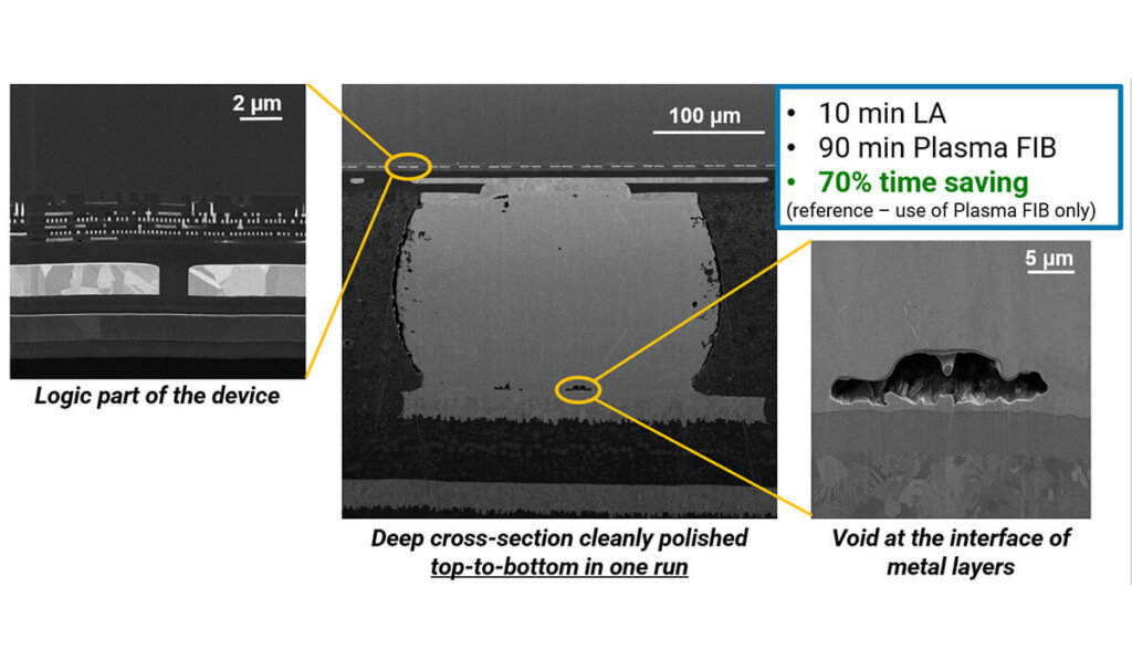
 Figure 3 (right) shows a cross-section several hundred micrometers deep and wide through a stack of through silicon vias (TSV) in a high bandwidth memory (HBM) device. It illustrates the ability of the system to cut a precisely vertical cross-section that passes through the center of each of the TSVs. Tilting the sample during laser ablation to compensate for taper angle was critical in reducing the amount of material to be removed by the final Plasma FIB milling operation, and thereby, the total time required for the cross-section. The cross-sectioning took 10 minutes in the laser ablation tool and 120 minutes in the Plasma FIB, an 80% time-savings compared to Plasma FIB alone.
Laser ablation preparation for FIB Tomography
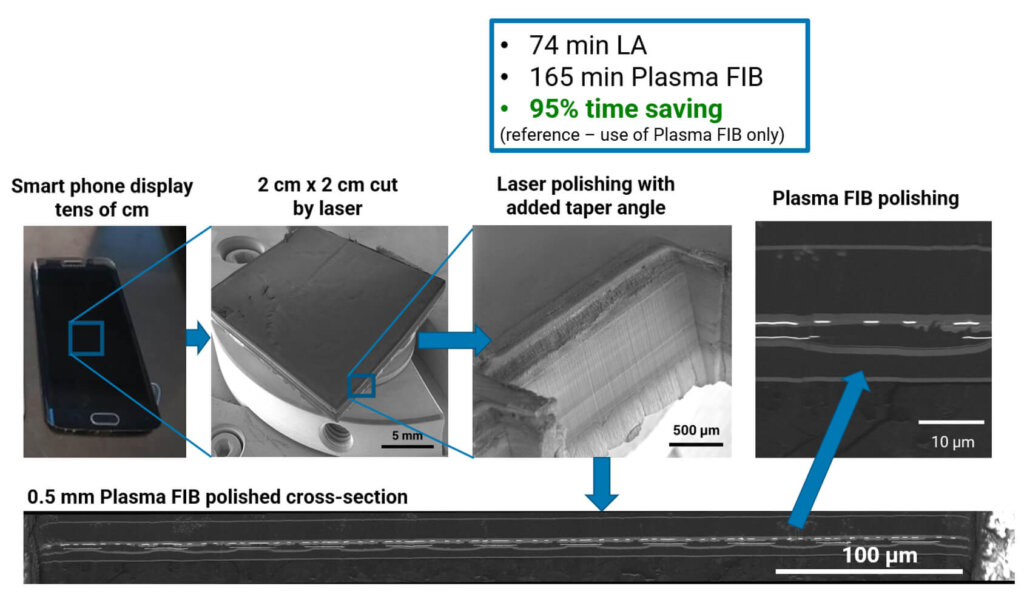
AMOLED Display
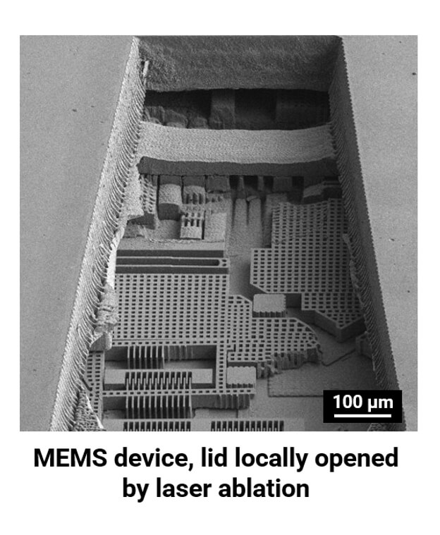
MEMS device
Summary
The use of advanced heterogeneous integration and packaging processes that interconnect multiple dies in a single package is growing rapidly. Analyzing failures in these packages typically requires the site-specific removal of overlying material to expose the suspect circuitry for inspection and analysis. The amount of material to be removed can be large.
![[err-ad-fallback-title]](http://www.3dincites.com/wp-content/plugins/a3-lazy-load/assets/images/lazy_placeholder.gif)
Although FIB systems have the precision needed to target specific circuit elements, they are slow, especially when using a Ga source. Plasma FIB is much faster but still could be perceived slow for large cross-sections needed in the advanced heterogeneous integration and packaging. Laser ablation is fast but not precise enough to target individual circuit elements with nanometer precision. Using laser ablation to remove the bulk of the material and FIB to clean and polish the final cross-section can greatly reduce the total time needed for the preparation. Systems that embed the laser ablation capability within the FIB system are inherently inefficient since only one capability can be used at a time.
The latest iteration of this technology implements parallel processing in stand-alone laser ablation and Plasma FIB tools, improving throughput and productivity by allowing processing in both tools at the same time. The tools are integrated through correlative image alignment procedures and CAD overlay navigation. In the parallel configuration, a single laser ablation system can feed multiple FIBs and other FA tools. This approach has the additional advantage of eliminating the risk of contaminating the FIB system, where contaminants can interfere with imaging and analysis or damage the system. We have shown several examples of large, high-quality cross sections and calculated time savings compared to preparation with Plasma FIB alone. Time savings in the examples shown ranged from 70% to > 95%.


Comments are closed.