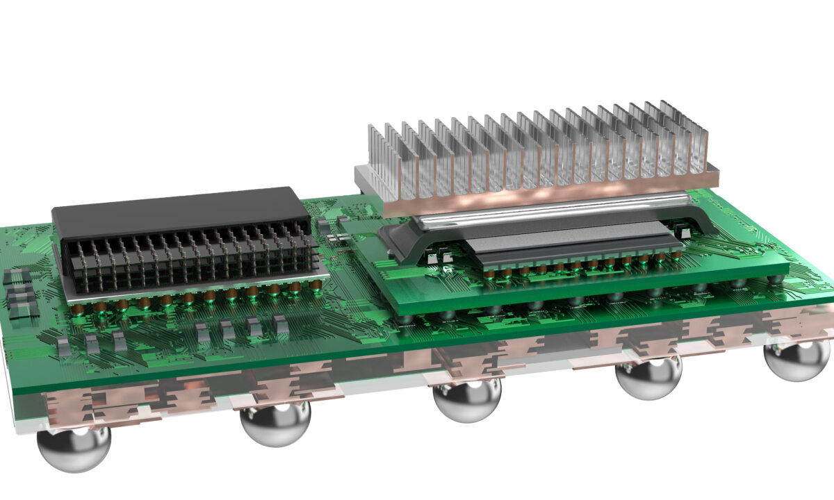
Advanced packaging has continued to evolve with various interconnect technologies on their way towards heterogeneous integration. Different assembly processes are used to optimize the yield of advanced packages, while the development of innovative advanced packaging materials is needed to address the many challenges faced in the assembly process for System in Package (SiP) and miniaturized modules.
Challenges for Advanced Packaging Materials
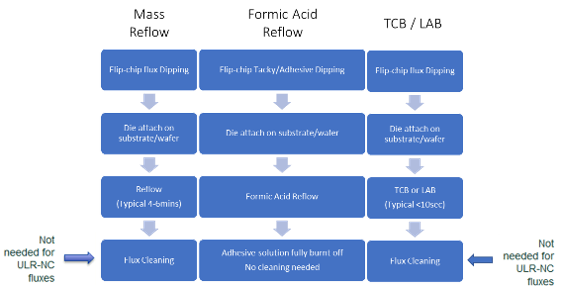
Larger die sizes with densely packaged interconnects – and the associated tighter pitches and smaller bumps – present challenges in the assembly process, including warpage-induced open joints and flux residue removal challenges due to the tight spacings, among others. For example, warpage from a larger and thinner silicon die and a thin substrate, along with an asymmetrical bump design, presents a common challenge to achieving a good yield in packaging. Thermo-compression bonding (TCB), laser-assisted bonding (LAB), and formic acid reflow without flux are used to overcome these challenges (Figure 1). TCB and LAB processes usually hold the wafer or substrate on a heated pedestal at 100-150°C for an extended period of time; if flux is used for the bonding process, this condition may cause a cleaning challenge for the hardened flux residue.
Hence, novel flux formulations and adhesive agents for wafer/die bonding have been developed. For example, the shift towards using semiconductor-grade ultra-low residue (ULR) no-clean flip-chip fluxes is one of the solutions to overcoming these challenges since the flux residue left behind after the soldering process is minimal (less than 10%, as low as 1%). The ULR flux has been utilized to eliminate the corrosion risk while providing adequate wetting and tack to form good joints without the need for cleaning, as the minimal flux residue is compatible with the underfill or molding materials used in the subsequent process.
For the formic acid reflow without flux (“fluxless”), a tacky or adhesive agent is used to hold the die in place during the process, and this tacky agent should not leave any residue that would be incompatible with the subsequent process.
For fan-out wafer-level packaging (FOWLP), typically a ball attach process is involved to form the interconnect bump. Other than the warpage issue and effectiveness of the flux removal process mentioned above, compatibility with new dielectric polymer coatings of polyimide, BCB, and PBO is another area of concern. Delamination and residue on the dielectric layer are some of the common issues due to the incompatibility between the different materials under the influence of temperature. After a thorough study of the interaction between the flux material and the dielectric layer at different temperatures, new flux materials have been developed that are compatible with the new dielectric polymer coatings.
Challenges in SiP
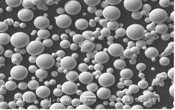
The deposition of solder paste for high-density SiP applications has become very challenging. In response to the miniaturization and functional densification of semiconductor packages for SiP and heterogeneous integration, a comprehensive portfolio of solder paste designed for ultrafine-pitch printing has been developed with fine powders ranging from Type 6 to Type 8 (Figure 2), by overcoming the oxidation challenges due to the large surface area of fine powders. For fine feature solder paste applications down to 100µm or less, the quality of fine solder alloy powder, flux formulations, and solder paste rheology are crucial to achieving consistent solder paste deposition and good soldering performance. These important features help reduce voiding and slumps with consistent printing performance, combining superior wetting performance with excellent stencil print transfer efficiency to satisfy the broadest range of process requirements. For certain packaging designs where the printing of solder paste may not be possible, micro-dispensing or precision jetting can also be used as an alternative, with consistent deposition down to 80µm feature sizes.
The development of new solders is also a critical enabler for heterogeneous integration. Alloys with different melting temperatures may be needed for SiP when there are different reflow cycles that require a solder hierarchy. In addition, lower melting temperature solders can provide better warpage control, especially for thin die/substrates, as well as minimized heat exposure for heat-sensitive components. Alloys with enhanced reliability have also been developed for automotive modules and other demanding applications.
Power Electronics & Thermal Management
A portfolio of materials solutions has been developed for power electronics, including low Alpha high-Pb solder paste with reduced leakage current for high power devices (e.g., GaN), and Durafuse™ HT (patent pending) using mixed solder powder technology as a high-temperature Pb-free alternative, which offers bond shear strength, thermal cycling reliability, and thermal conductivity better than (or at least comparable to) high-Pb, while using soldering processes similar to the current high-Pb soldering process.

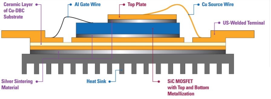
Developments in Ag and Cu sintering paste formulations have resulted in solutions for die-attach, package attach, and similar applications for power electronics (Figure 3) with significantly enhanced properties, including bond shear strength and thermal conductivity. The high metal loading materials are designed to leave minimal organic residue after the sintering process, with fast sintering and strong joint strength for pressureless and pressurized sintering, on different surface finishes (e.g., Ag, Cu, and Au). Low voiding and porosity have been achieved with pre-dry and pressure-assisted sintering processes.
To address the thermal management challenges as the power density of semiconductor devices increases and the junction temperature rises, multiple thermal interface material (TIM) solutions with a wide range of thermal conductivity and forms have been developed over the years. Metal TIMs are increasingly being used in demanding applications, including indium-based TIMs and gallium-based TIMs. It is interesting to note that gallium-based liquid metal TIMs are opening up new possibilities in thermal management, due to their robust wetting properties with various surfaces and the promise of eliminating “leakage.”
Summary
Methodical development, proper selection, and application of advanced packaging materials for the various assembly processes are crucial to ensuring high production yield for the assembly process for advanced packaging and SiP applications. For further information, please contact Dongkai Shangguan.