
Herb News - Page 3
Reaping the Benefits of a Design and Manufacturing Ecosystem
As it does each year, TSMC recently brought 45 of its ecosystem partners together for its annual Open Innovation Platform®...
A Look at US Investments in Heterogeneous Integration
The semiconductor industry is not only very capital-intensive, but investors experience very long payback times. Both limit the availability of...
The Path to Smarter Fabs
Working from the mantra “None of us knows as much as all of us,” SEMI invited manufacturers of electronic components...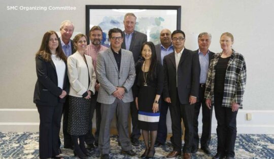
The Importance of Fully Characterized Semiconductor Materials
More than 20 years ago, the cooperation between fabless IC vendors and wafer foundries started to dominate over the integrated...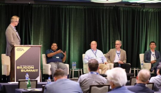
The Need For and Value of Semiconductor Industry Organizations
Recognizing the need fand value of semiconductor industry organizations, in 1994, Jodi Shelton and CEOs of fabless IC companies founded ...
How to Transform Innovative Technologies Into Customer-Specific Solutions
Technology innovations don’t reach customers right away. Since 1980 I have observed how our industry has improved key parameters like...
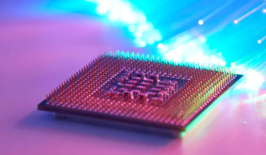
What is Happening to the Memory Market?
Because memory represents typically about half the silicon content of a system, and multi-die packages typically combine many memory devices...
Advanced SiPs Help More than Moore Reach Maturity
Earlier this summer, 175 system-in-package (SiP) experts from all over the world met at the Marriott Hotel in Monterey’s Old...New Details About More-than-Moore Test Technology Advances
SEMICON West and the Electronic System (ES) Design West were, for the first time, co-located at the Moscone Center in...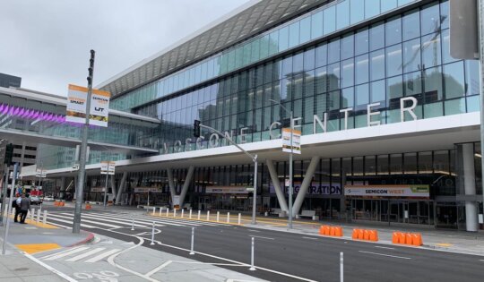
SEMICON West Keynotes Look to a Future Beyond Moore’s Law
In addition to Francoise’s post about technology megatrends here, below is part one of my perspective, mostly about the SEMICON West...
The Importance of a Well-coordinated Semiconductor Supply Chain
Would you buy your next hotdog in parts, from un-coordinated suppliers? For example: Get the bun from a baker, the...
Book Review: Handbook of 3D Integration – Volume 4
An essential part of successfully introducing a new technology is to educate engineers and managers on its benefits and tradeoffs....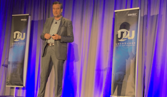
U2U 2019 Conference Dives into 2.5/3D IC Design
Key advanced packaging technology influencers came out in force to discuss the status of EDA tools for 2.5D/3D IC package...
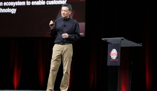
TSMC’s 2019 Technology Symposium highlights 25 Years of Innovation
In 1994 TSMC, a small wafer foundry from Taiwan held its first Technology Symposium. Since 1999 I have had the...
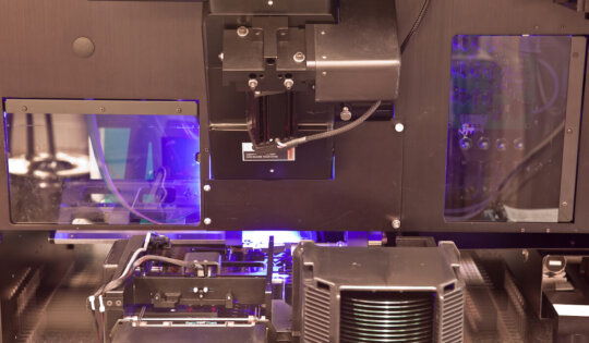
Update on 3D X-ray and DBI Technology for Advanced and 3D Packaging
The Microelectronics Packaging & Test Engineering Council (MEPTEC) held its monthly meeting at SEMI in Milpitas on April 10. Two...
DesignCon 2019 Shows Board and System Designers the Benefits of Advanced IC Packaging
Santa Clara’s Convention Center was home to DesignCon 2019 from January 29-31, 2019. This conference is well known for showing...
ISS 2019 Continued: Facing New Challenges and Opportunities
Just in case you didn’t have a chance yet to read part 1 of the ISS 2019 blog, covering day...
ISS 2019: Semiconductor Industry Faces New Challenges and Opportunities
SEMI held its annual Industry Strategy Symposium (ISS 2019) at the Ritz Carlton in Halfmoon Bay, CA January 6-9, 2019....