

An essential part of successfully introducing a new technology is to educate engineers and managers on its benefits and tradeoffs. That’s why Wiley started publishing the Handbook of 3D Integration Series with Volume 1 and 2 in 2008, followed by Volume 3 in 2014. This blog covers Volume 4, introduced in early May 2019. It focuses on three important 3D challenges: IC design, test, and thermal management. It conveys what 3D ICs can do today and gives advice on how to best utilize these capabilities profitably.
Setting the Stage
For the last 50+ years, Moore’s Law has enabled the semiconductor industry to offer, with every new process node, higher performance, and lower power at a lower cost per function. However, as IC development cost, design times and production ramp-up challenges for large designs have been increasing significantly, only very high-volume and high-margin applications can now pay back the enormous investments needed to continue following Moore’s Law. These and stepper-field limitations clearly constrain how much functionality designers can pack into a single-die IC.
In addition to these challenges on the suppliers’ side, market requirements have changed significantly. Now, most applications demand that semiconductor vendors deliver, within a few months and not years, larger and larger system building blocks. These blocks need to contain, in addition to lots of digital logic, a significant amount of memory, often analog and/or RF functions, even MEMS and sensors. These requirements clearly exclude the traditional single-die system-on-Chip (SoC) approach from many applications and suggest focusing on a much more flexible methodology to integrate lots of digital and heterogeneous functions. It’s called system-in-package (SiP). (Comment: In this blog SiP, 2.5D, 2.5/3D, 3D and multi-die IC are often used interchangeably.)
SiP solutions, a.k.a. multi-chip modules (MCMs), have been available for many years, but their relatively high cost and inadequate design tools support have limited their deployment to less cost-sensitive applications and limited their complexity. The increasing market pressure for cost-effective integration of more digital and heterogeneous functions has motivated many IC design tools and manufacturing companies to develop solutions for design and manufacturing of lower cost multi-die ICs — generally called 3D ICs.
Handbook of 3D Integration: Design, Test and Thermal Management
Design
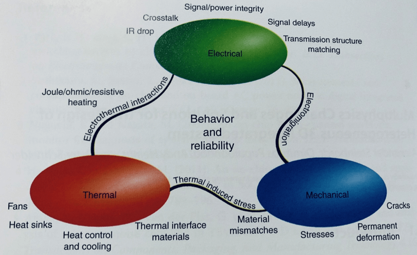
The first part of the Handbook of 3D Integration, Volume 4, (Chapters 1 to 8), edited by North Carolina State University (NCSU) Professor Paul D. Franzon, covers 3D IC design topics. Franzon and several other experienced 3D IC design experts contributed to the wide range of 3D IC topics designers need to know about. In addition to 3D IC basics, these chapters outline why and how to partition a design into multiple dice, (a.k.a. pathfinding step), but also dive into considerations for die placement and orientation and how to interconnect them with micro-balls and through-silicon-vias (TSVs). Chapter 3 explains the important points for implementing the power distribution network (PDN). Chapter 4 addresses coupling between individual TSVs and the redistribution layers (RDLs) as well as the many electrical-thermal-mechanical interactions in a multi-die IC that designers need to consider (Figure 1).
In view of all these multi-physics challenges, the importance of utilizing electronic design automation (EDA) tools for planning, implementation, and verification of design, the interactions between dies and with the package in multi-die ICs becomes obvious. To accurately simulate these effects, accurate models of all multi-die building blocks and the behavior of materials is essential. See details in Chapter 18.
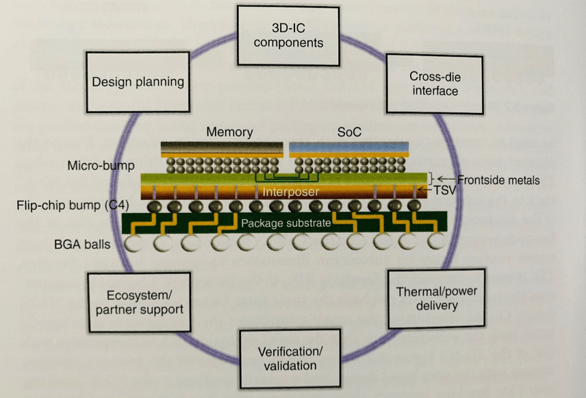
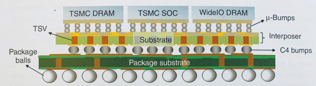
In Chapter 5, an experienced engineering team from TSMC describes their reference flow and other considerations for utilizing the CoWoS® interposer technology (Figure 2).
Chapters 6 talks in more depth about individual design steps and EDA tools. Chapter 7 dives more into design flows. Several application examples demonstrate architectural benefits and trade-offs that need to be considered when integrating multiple dies into one IC package. When a large amount of memory and logic are needed for a high-performance design, multi-die ICs clearly offer the best way to break down the dreaded “memory wall”.
That’s why Chapter 8 is dedicated to explaining high-bandwidth memories (HBMs), DRAM architectures, controllers, memory modeling and the challenges when combining memory and logic dies on an interposer.
The summary of every chapter in this book is followed by a long list of references for related design topics. This allows readers to quickly and easily dive much deeper into topics of interest.
In addition to the wide range of benefits and challenges described in the design section above, two other topics also deserve very specific attention, because they significantly impact unit cost, performance and quality/reliability of multi-die ICs too. These topics are test and thermal considerations. Test is covered in depth in Chapters 9 to 15, while Chapters 16 to 19 focus on thermal management.
Test
The second part of this book was edited by Erik Jan Marinissen, Scientific Director at imec in Leuven, Belgium.
Observability and controllability are important criteria to enable exhaustive testing and ensure high yields and reliable products. When combining multiple dies in a package, physical access to individual dies gets limited, especially when these dies are vertically stacked. Test experts in the planning/design and manufacturing/test camps have been working together for more than a decade, to improve testability, yield and quality/reliability of multi-die ICs, while minimizing cost. This part of Volume 4 covers many of the innovations made to date and recommends where and how to apply them.
Figure 3 compares a traditional single die test flow with test requirements for multi-die ICs, where “n” is the number of individual dies (including interposer!) to be integrated into a package.
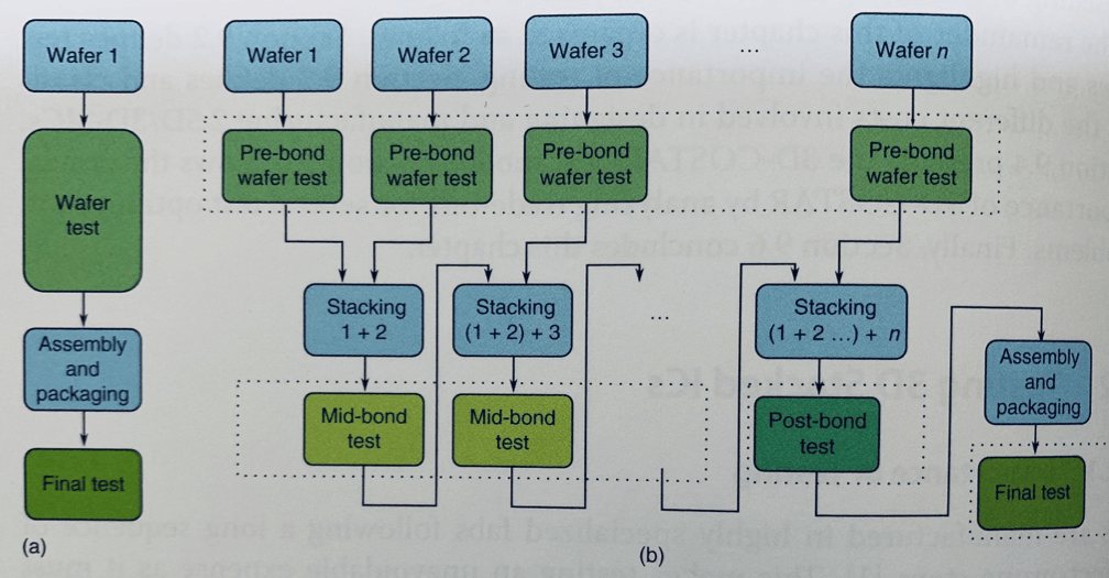
In addition to the test steps shown in Figure 3, die need to be designed for test (DFT) to achieve good results. Also, in addition to testing all dies, passive and active interposers, passive components mounted on interposers or package substrates as well as the interconnections between all these dies and other components and the package pins need to be tested as well.
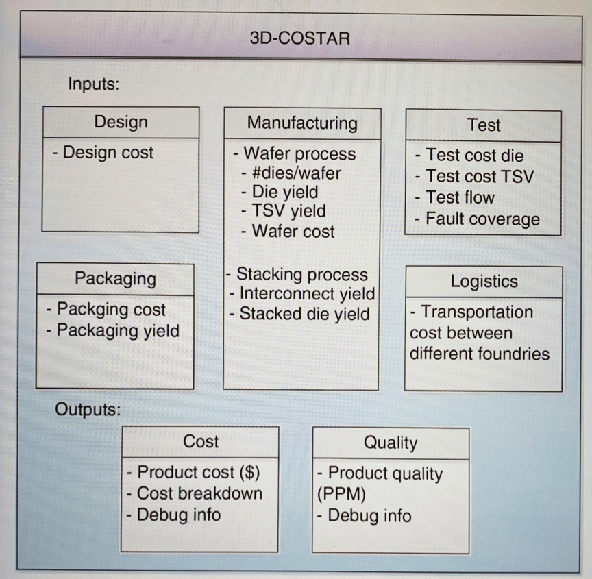
In addition to the importance of test, Chapter 9 also describes 3D-COSTAR, a newly developed, comprehensive cost model for 3D IC test. It allows users to evaluate if adding more design for test (DFT) features (e.g.: probe-pads, built-in self-test) or adding more test steps and increasing the test time is more cost-effective.
Chapter 10 conveys many ideas for testing interconnects in multi-die ICs for failures like bridging or opens, as well as leakage, high resistivity, excessive capacitance and other failures impacting performance.
“known good die” (KGD) has been a research topic for IC design and test experts for many years.

Chapter 11 covers advancements in the development and use of probe cards, to improve pre-bond testing. The next chapter recommends DfT architectures, test data compression (DTC) techniques, how to test embedded cores and what to consider for at-speed testing of multi-die ICs.
Chapter 12 also suggests how to test the interactions between logic stacks and memories. It also explains the approved IEEE and JEDEC standards covering 3D ICs. The following chapter cover optimization of test-access architectures and scheduling for 3D ICs.
Chapter 14 concentrates on the IEEE P 1838 standard in development and explains how it utilizes facilities and features of IEEE 1149.1, 1500 and 1687, for testing of single and multi-tower stacks and interposers.
Chapter 15 uses a TSMC CoWoS design (Figure 5) to describe the test and debug strategies for heterogeneous designs and also explains passive interposer test considerations.
Thermal Management
Last, but certainly not least, Part III, of Volume 4 focuses on heat management alternatives. Edited by Muhannand S. Bakir from Georgia Institute of Technology (a.k.a. GeorgiaTech), Chapters 16 to 19 address this important and challenging aspect of 2.5/3D IC design.
Packing multiple dies closely together in an IC increases performance. In addition, it allows scaling back the size of most I/O buffers, cuts interconnect lengths and parasitic capacitances by several orders of magnitude. It has demonstrated to reduce total power dissipation (Watts), compared to single-die SoCs, mounted on a printed circuit board (PCB), to about one third when using interposers and even more when stacking dies vertically. However, power density (Watts per cm3) increases significantly, due to the much smaller form-factor of a multi-die IC, compared to the equivalent functionality, mounted on a PCB.
Chapter 16 describes a wide range of thermal challenges. It explains methods to isolate heat sensitive components from other dies, generating significant heat and describes cooling techniques, including microfluidic cooling, to conduct heat away from active and passive components in a multi-die IC.
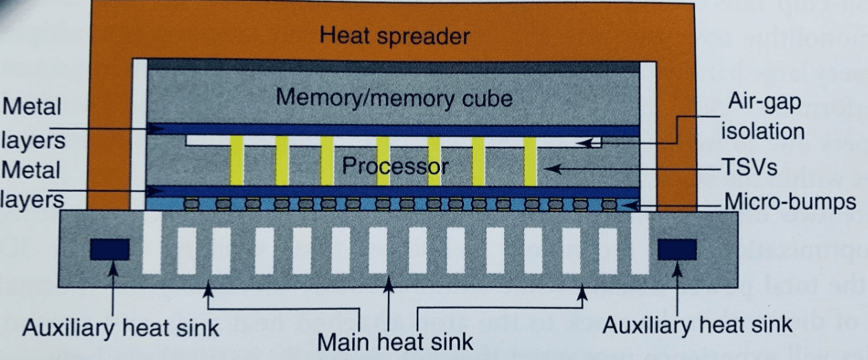
Figure 6 shows how a high-power processor die, mounted on an interposer or substrate, is being cooled with microfluidic channels underneath. The airgap above isolates a heat sensitive memory, from the heat generated by the logic die below. Also, the heat spreader on top cools the memory. Sub-chapters 16.1 to 16.5 address these topics in depth and describe many cooling methods.
To predict the temperatures of individual components in a multi-die IC, the generated heat needs to be summarized. Then designers need to consider all thermal paths and their capability to conduct heat out of the 3D IC and into the package, board, and system. Chapter 17 describes how to evaluate passive and active cooling techniques. and how to calculate the effectiveness of cooling liquids, air, and solid-state cooling techniques.
Chapter 18 describes thermal modeling and model validation techniques for vertically stacked dies in 3D ICs. For many designs, compact models may suffice. For more complex designs finite element modeling (FEM) or computational fluid dynamics (CFD) methods need to be applied, to generate accurate models and also enable full-chip layout-based thermal simulations. This chapter also describes how to design thermal test vehicles.
Chapter 19 talks in-depth about the important role of thermal interface material (TIM) and how micro-channels in cold plates can be used for single-phase or the very effective two-phase cooling.
Starting on page 461, a keywords index makes accessing needed topics quick and easy.
Thoughts and Observations
- In the last ten years, many leading-edge companies have demonstrated the ability of 2.5D designs to increase performance per Watt by 3X and more.
- Stacked memory dies in 3D ICs have enabled designers to break down the dreaded Memory Wall.
These and emerging technology advancements will allow semiconductor vendors to offer application-specific, system-level building blocks to increase their valuable contributions to system designers and their own profits.
The latest edition of the Handbook of 3D Integration clearly offers you a great opportunity to expand from the current, mostly component-driven business model to higher value system-level solutions.
I hope to meet you at the IMAPS conference in Monterey, CA, late June, as well as at both ES Design West and Semicon West, co-located in San Francisco early July.
Thanks for reading this very long blog…….Herb


