 Multichip module (MCM), system-in-package (SiP), system-on-chip (SoC), and heterogeneous integration are all important semiconductor packaging technologies. They deserve to have, at the very least, a book written about them. However, herein I would like to give these technologies very simple descriptions. if you don’t mind.
MCM
MCM integrates different chips and discrete components side-by-side on a common substrate (either ceramic, silicon, or organic) to form a system or subsystem for high-end networking servers and computer applications.
MCM-C are multichip modules that use thick film technology such as fireable metals to form the conductive patterns, and are constructed entirely from ceramic or glass-ceramic materials, or possibly, other materials having a dielectric constant above five. In short, an MCM-C is constructed on ceramic (C) or glass-ceramic substrates [1].
MCM-D are multichip modules on which the multilayered signal conductors are formed by the deposition of thin-film metals on unreinforced dielectric materials with a dielectric constant below 5 over a support structure of silicon, ceramic, or metal. In short, MCM-D uses deposited (D) metals and unreinforced dielectrics on a variety of rigid bases [1].
MCM-L are multichip modules which use laminate structures and employ PCB technology to form predominantly copper conductors and vias. These structures may sometimes contain thermal expansion controlling metal layers. In short, MCM-L utilizes PCB technology of reinforced organic laminates (L) [1].
There was much research performed on MCMs during the 1990s. Unfortunately, at that time, due to the high-cost of ceramic and silicon substrates and the limitation of line width and spacing of the laminate substrate, the high volume manufacturing (HVM) of MCMs never materialized. Actually, since then, MCM has been a “dirty” word in semiconductor packaging.
SiP
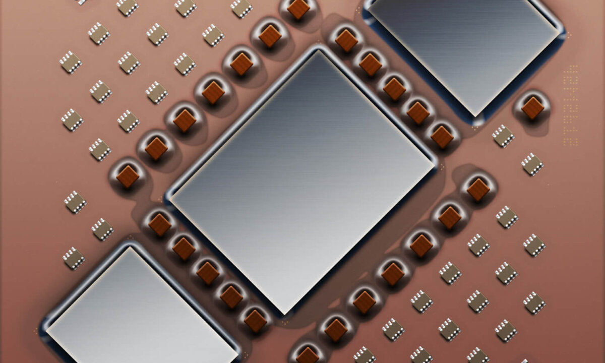
SiP integrates different chips and discrete components, as well as 3D chip stacking of either packaged chips or bare chips (e.g., wide-bandwidth memory cubes and memory on logic with through silicon vias (TSVs)) side-by-side on a common (either silicon, ceramic, or organic) substrate to form a system or subsystem for smartphones, tablets, high-end networking server and computer applications. SiP technology performs horizontal as well as vertical integrations. Some people also called SiP vertical MCM or 3D MCM.
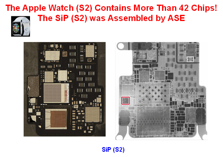
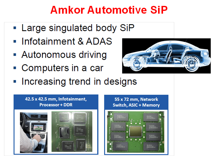
Unfortunately, because of the high cost of TSV technology [2, 3] for smartphones and tablets, it never materialized. Most SiPs that went into HVM in the past 10 years are actually MCM-L for low-end applications such as smartphones, tablets, smart watches, medical, wearable electronics, gaming systems, consumer products and internet of things (IoT) related products such as smart homes, smart energy, and smart industrial automation. Usually, the SiPs integrate two or more dissimilar chips and some discrete components on a common laminated substrate. Some SiP examples are shown in Figures 1 and 2 below.
The applications of SiP for the high-price, high-margin, and high-end products are, e.g., dual-lens camera modules. However, right now this SiP cannot be all done by the OSATs, but also involves optical design, testing, lenses, micro-motors, flexible substrate, and system integration capabilities which still need to be strengthened.
SoC
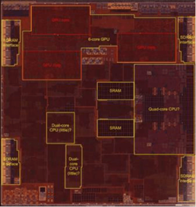
SoC integrates ICs with different functions into a single chip for the system or subsystem. Because of the drive of Moore’s law, SoC has been very popular in the past 10+ years. For example, Apple’s application processor (AP) A10 consists of a 6-core GPU (graphics processor unit), two dual-core CPU (central processing unit), 2 blocks of SRAMs (static random access memory), etc. as shown in Figure 3. The A11 is using the 10nm processing technology for the HVM by TSMC and scheduled to be shipped in September this year. The A12 is most likely to be fabricated by TSMC’s 7nm processing technology in 2018.
Heterogeneous Integration
Heterogeneous integration [4, 5] is against SoC but very similar to MCM/SiP. It has been a very “fancy” name in semiconductor packaging in the past few years. This is because the end of Moore’s law is fast approaching and it is more and more difficult and costly to reduce the feature size (to do the scaling) to make the SoC.
People (for example, COO of ASE, Dr. Tien Wu on March 6, 2017 [6]) are talking about using packaging technology to integrate the dissimilar chips with different functions instead of integrating all the functions into a single chip and go for finer feature size. For the next five years, we will see a higher level of heterogeneous integration, whether it is for performance, form factor, power consumption or cost.
Four months ago (April 3, 2017), Apple announced it would begin making graphics chip designs in house and cut off its reliance on Imagination Technologies within two years. (Note: Imagination Technologies has licensed high-performance graphics processor unit (GPU) designs, known as PowerVR graphics series, for use in Apple’s A-series dating back to the original iPhone in 2007. Apple licenses the PowerVR series of GPUs and combines them with memory, logic and ARM-based CPU parts on to a single SoC.)
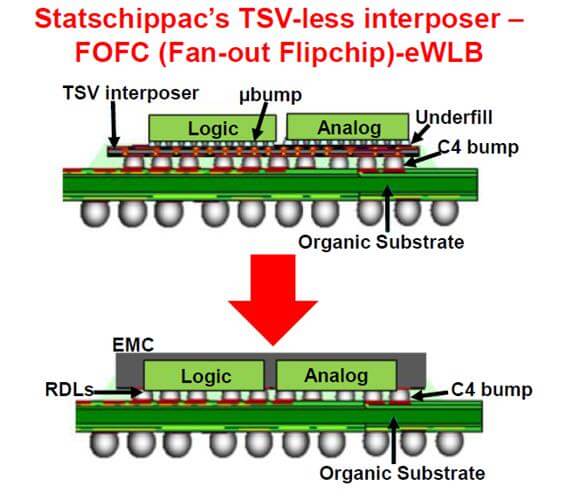
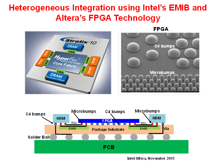
All these indicate that heterogeneous integration is going to take market share away from SoC on high-end applications such as the high-end smartphones, tablets, wearables, networkings, telecommunications, and cloud computing. How to let these dissimilar chips talk to each other? Redistribution layers (RDLs) [7]! These RDLs can be fabricated by such as fan-out wafer-level packaging (FOWLP) technology [8-11] as shown in Figure 4 by STATsChippac, embedded multi die interconnect bridge (EMIB) [12] technology as shown in Figure 5 by Intel, and many other TSV-less interposers [13].
A Final Note:
I’m going to teach a workshop, Fan-Out Wafer-Level Packaging and 3D Packaging (WS7), on Sunday. September 17, 2017 from 1:30PM to 5:00PM, as part of the 2017 SMTA International Technical Conference to be held at the Donald E. Stephens Convention Center, Rosemont, IL, from September 17-21, 2017. Please join us by registering here. If you registered before August 25, you will have 10% off. ~ JHL
![[err-ad-fallback-title]](http://www.3dincites.com/wp-content/plugins/a3-lazy-load/assets/images/lazy_placeholder.gif)
References
[1] Lau, J. H., COB Technologies for MCMs, ITP Book Company, New York, 1994.
[2] Lau, J. H., Through-Silicon Vias for 3D Integration, McGraw-Hill Book Company, New York, 2013.
[3] Lau, J. H., 3D IC Integration, and Packaging, McGraw-Hill Book Company, New York, 2016.
[4] Iyer, S. S., “Heterogeneous integration for performance and scaling,” IEEE Trans. Components, Package. Manuf. Technol., vol. 6, no. 7, 2016, pp. 973–982.
[5] Bajwa, A. A., S. Jangam, S. Pal, N. Marathe, T. Bai, T. Fukushima, M. Goorsky, and S. S. Iyer, “Heterogeneous Integration at Fine Pitch (≤ 10μm) using Thermal Compression Bonding”, IEEE/ECTC Proceedings, June 2017, pp. 1276-1284.
[6] https://semiengineering.com/what-next-for-osats/, March 6, 2017.
[7] Lau, J. H., P. Tzeng, C. Lee, C. Zhan, M. Li, J. Cline, et al., “Redistribution layers (RDLs) for 2.5D/3D IC integration,” Proc. of IMAPS Symp., 2013, pp. 434-441. Also, IMAPS Trans., Jour. Of Microelectronic Pckging., 2014, pp. 16-24.
[8] Yoon, S., P. Tang, R. Emigh, Y. Lin, P. Marimuthu, and R. Pendse, “Fanout Flipchip eWLB (Embedded Wafer Level Ball Grid Array) Technology as 2.5D Packaging Solutions”, IEEE/ECTC Proceedings, 2013, pp. 1855-1860
[9] Lin, Y., W. Lai, C. Kao, J. Lou, P. Yang, C. Wang, and C. Hseih, “Wafer Warpage Experiments and Simulation for Fan-out Chip on Substrate”, IEEE/ECTC Proceedings, 2016, pp. 13-18.
[10] Chen, N., T. Hsieh, J. Jinn, P. Chang, F. Huang, J. Xiao, A. Chou, and B. Lin, “A Novel System in Package with Fan-out WLP for high-speed SERDES application”, IEEE/ECTC Proceedings, 2016, pp. 1495-1501.
[11] Fukushima, T., A. Alam, Z. Wan, S. C. Jangam, S. Pal, G. Ezhilarasu, A. Bajwa, and S. S. Iyer, “FlexTrate – Scaled Heterogeneous Integration on Flexible Biocompatible Substrates using FOWLP”, IEEE/ECTC Proceedings, June 2017, pp. 649-654.
[12] Mahajan, R., R. Sankman, N. Patel, D. Kim, K. Aygun, Z. Qian, et al., “Embedded multi-die interconnect bridge (EMIB) – a high-density, high-bandwidth packaging interconnect,” IEEE/ECTC Proceedings, 2016, pp. 557-565.
[13] Lau, J. H., “TSV-less Interposers”, Chip Scale Review, Vol. 20, September/October 2016, pp. 28-35.