
 As it does each year, TSMC recently brought 45 of its ecosystem partners together for its annual Open Innovation Platform® Forum to demonstrate to joint customers the value of a well-managed IC design and manufacturing ecosystem. TSMC and many of the partners presented recent accomplishments and explained in 33 technical papers how they support customers in today’s challenging markets for electronic products.
Lessons Learned from the Automotive Manufacturing Ecosystem
Starting with Henry Ford’s Model T, introduced on October 1, 1908, (exactly 111 years ago) the automotive industry has built and matured an ecosystem to design, manufacture, improve productivity, quality and reliability as well as achieve much lower unit cost. Now most of us can afford an economical, reliable and stylish car, because many companies, each focused on their field of expertise, work together. Customers also benefit from better products while suppliers achieve higher sales volumes in this ecosystem. TSMC’s OIP follows the same strategy and has, in its first 10 years, demonstrated remarkable technical progress and offered customer benefits.
In his welcome remarks, Dave Keller, President and CEO of TSMC North America, conveyed several important data points impacting the semiconductor manufacturing ecosystem:
- 18 5G networks are deployed worldwide today
- TSMC engineers are certified on major standards to support the automotive industry’s drive for save, smart and green vehicles
- High-performance computing chips from TSMC apply artificial intelligence (AI) and machine learning (ML) to analyze increasing amounts of sensor data
- TSMC’s Grand Alliance now includes equipment and materials vendors
- TSMC remains committed to being a pure-play foundry
TSMCs Technology Toolbox
Dr. Cliff Hou, VP of Technology Development for TSMC, shared his speaking slot with Dhiraj Mallik, VP Engineering and Business Development at Cerebras Systems. Hou highlighted three pillars TSMC relies on to serve customers:
- Advanced technology (N7, N6, N5, …)
- Specialty technology (ULL, RF, BCD,…)
- 3DIC technology (SoIC, InFo, CoWoS,…)
He confirmed that N7+ has been in production since April 2018 thanks to extreme ultraviolet {EUV) lithography. Additionally, cost-reduced N6 is design-rule compatible and available for risk-starts in 1Q/2020. Several of his slides outlined speed, power and density advantages of N5 versus N7, detailed the available library elements for N5, and the steps of the design for which major EDA vendors are qualified.
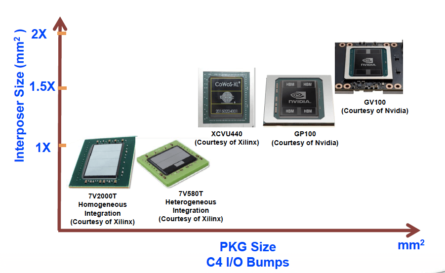
Hou also talked about TSMC’s specialty technologies for low power, high voltage, and RF. He mentioned that chip-on-wafer-on-substrate (CoWoS) interposers are getting larger (Figure 1)( and larger and that organic interposers enable lower-cost integrated fan-out (InFO) designs. Hou topped his message with a slide showing TSMC’s approach to integrating chiplets and announced the development plans for 5G platforms and other applications.
Mallik’s presentation brought me initially back to the not so good old days of Trilogy’s wafer-scale integration. After he explained how his 200 person team uses an entire TSMC N16 wafer to pack 1.2 Trillion transistors, 18 GBytes of on-chip SRAM and lots of smart interconnects together and, thanks to its architecture and the benefits of redundancy, makes this gigantic circuit function well, I find wafer-scale integration very promising.
Focus on Advanced Packaging and Design Enablement
Dr. Douglas Yu, Vice President of Integrated Interconnect & Packaging as well as Suk Lee, TSMC Senior Director, Design Infrastructure Management Division, gave overviews of their respective fields of expertise.
Yu confirmed that TSMC provides silicon interposers with up to 3X reticle size for CoWoS designs now and up to 1.5X for InFO designs soon. He emphasized that TSMC sees heterogeneous (multi-die) integration as a needed extension of Moore’s Law, and is committed to qualifying up to 10 chiplets (a.k.a. bare die, KGD,…) in a package soon.
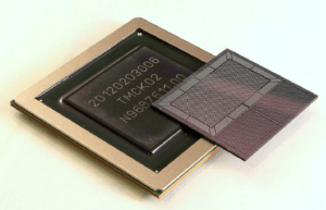
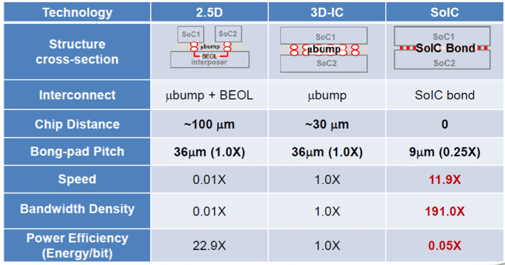
Yu explained different InFO configurations, e.g. InFO package-on-package (InFO PoP) and InFO on Substrate (InFO oS). TSMC offers capabilities for even tighter multi-die integration. Their system-on-IC (SoIC) technology deploys wafer-to-wafer or die-to-wafer stacking (in the fab) and utilizes fine-pitch copper wiring (figure 3).

Instead of using the relatively large micro-bumps allowing 800 interconnects/mm2 in 2.5D and 3D-ICs, TSMC connects vertically stacked die in SoICs with tiny copper bonds. This bump-less SoIC technology offers a bond-pad pitch of only 9 µm today and allows up to 1.2 Million interconnects/ mm2. Yu mentioned that the HBM 2 family uses a 50 µm pitch today. The HBM3 versions will offer a tighter pitch to also improve wiring density.
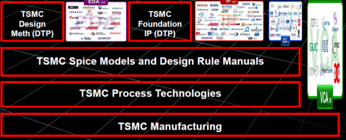
Suk Lee described how TSMC’s Design Enablement Division complements TSMC’s process and OIP partners’ capabilities by enabling customers to design with them. He pointed out that TSMC’s OIP Alliance is now 10 years old and comprises 42 IP partners, 22 EDA partners, 19 design services partners, seven value chain aggregators, and six cloud alliance partners. Lee explained that TSMC applies strict criteria to qualify these partners and every one of their contributions to the alliance for every process node. In addition, TSMC also monitors partners’ performance and takes corrective actions if/when/as needed. Figure 3 shows how TSMC and all its partners work together to serve customers.
Summary
Semiconductors are at the core of vehicles, phones, appliances, IoT edge notes, computers and networking equipment, and many other applications. To be competitive, these products need to provide a high enough value to the user – at an affordable price – then revenues and profits will follow. Providing enough value to a specific application requires designers with domain knowledge. Only a comprehensive design and manufacturing ecosystem – like TSMC has built – can meet these diverse and demanding requirements. TSMC’s revenues climbing to #3, behind Intel and Samsung, in 2019 semiconductor revenues confirms the value of strategic cooperation.
Thanks for reading …Herb
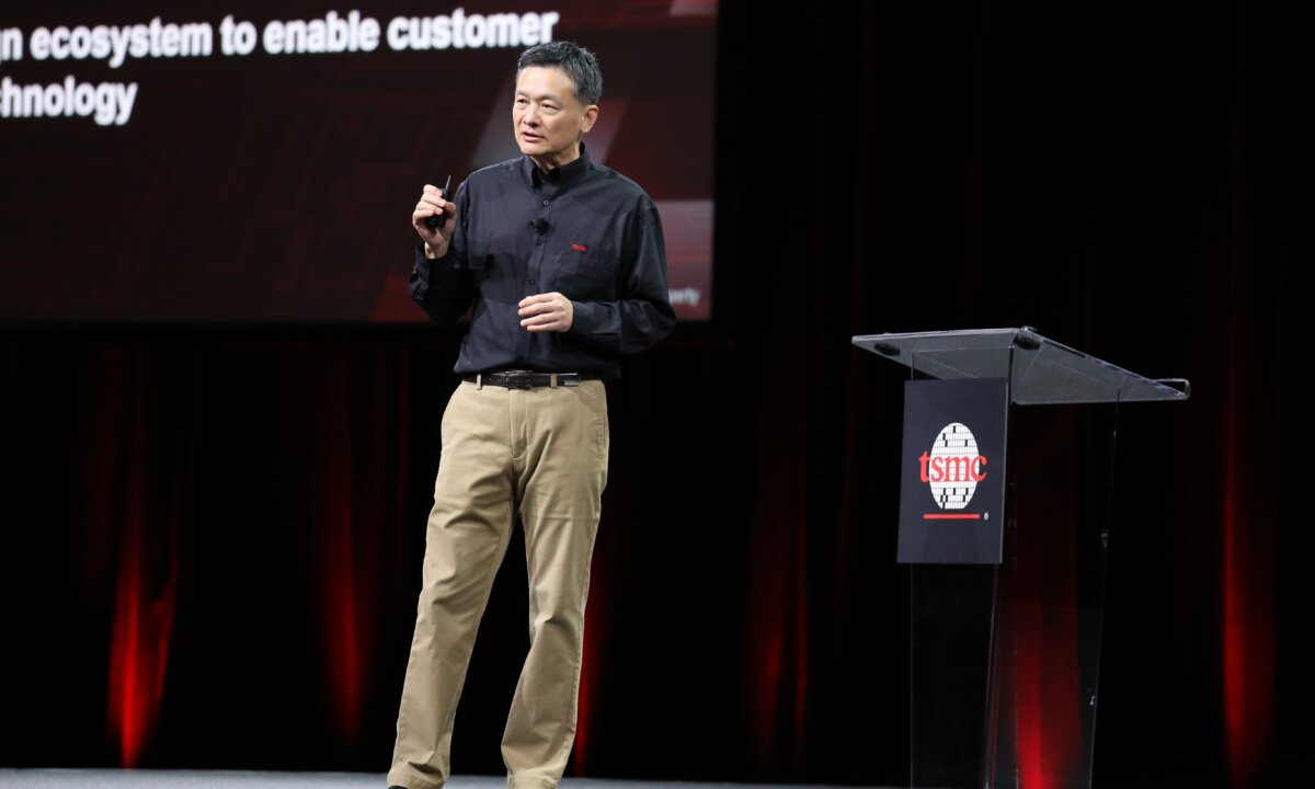
Feature photo: Dr. Cliff Hou, Vice President of Technology Development for TSMC (Source: TSMC)


