
 In 1994 TSMC, a small wafer foundry from Taiwan held its first Technology Symposium.
Since 1999 I have had the privilege to work with TSMC and closely follow their success in building a powerful and cost-effective ecosystem for the fabless IC vendors and foundry business model. To measure their success in hard numbers, please check IC Insights’ 2018 revenue estimates here and see that TSMC has a solid place within the top five semiconductor vendors.
25 Years, in Retrospect
Recognizing that System-on-Chip (SoC) technology has limits, In 2011, together with Xilinx, TSMC introduced its chip-on-wafer-on-substrate (CoWoS®). This 2.5D multi-die packaging technology targets high-performance designs and integration of heterogeneous functions in a package. In 2015 the company introduced integrated fan-out (InFO), its wafer-level technology, to offer multi-die packaging for cost-sensitive applications like iPhones.
This year, at their 25th Technology Symposium, TSMC highlighted its radio frequency (RF) solutions (killer-app 5G), various specialty processes (e.g. for automotive), further cost reductions with a 6nm process and many ways to improve performance per watt with their 7nm and 5nm technologies (e.g. for artificial intelligence (AI) chips).
Why am I taking you down memory lane? Have I gone senile? I hope you don’t think so!!!
All these big steps tell me that TSMC listens well to customer requirements and can execute in a timely fashion. In addition, TSMC complements its manufacturing prowess with many ecosystem partners to offer 1) user-friendly design enablement capabilities and 2) heterogeneous IP building blocks. All these are the foundation for creating applications-driven solutions for much higher levels of building blocks for electronic system design.
But enough about rear-view mirror observations and rapidly emerging new market requirements. Let’s focus on the 25th Technology Symposium TSMC held at the Santa Clara Convention Center on April 23rd.
TSMC Today
Dave Keller, President, and CEO of TSMC North America, welcomed more than 2000 attendees and proudly mentioned that last year, TSMC shipped 5438 products on six million 300mm wafers. He outlined the day’s agenda and encouraged us to visit TSMC’s experts at their main booth, their IC packaging, and the RF booth.
Dr. CC Wei, TSMC’s CEO, explained that 5G and AI will drive silicon demand for data collection and analysis. He reminded the audience that TSMC wants to be the trusted technology and capacity provider for the global IC industry and that 1300 design technology engineers at TSMC and more than 10,000 engineers at EDA and IP partners are ready to support customer engagements.
Wei summarized progress on the latest nodes:
- N7+ is in mass production with good yields
- N5 is offering better density and performance, due to more EUV layers, is ramping production
- N6 is offering better logic density than N7, can utilize the N7 IP portfolio and ramps in 1Q/2020.
Wei also highlighted the increasing market needs for adding specialty technology processes, like bipolar-CMOS-DMOS (BCD) a process technology for high current applications; non-volatile memory (NVM); high voltage (HV), CMOS image sensors (CIS), microelectromechanical systems (MEMS), RF, and low-power analog to meet the increasing needs for heterogeneous integration. Advanced IC packaging is, of course, essential for integrating such multi-die designs.
Victor Peng, president, and CEO of Xilinx represented this long-term TSMC partner. He outlined Versal, a 7nm nm product from the Xilinx family of adaptable computing acceleration platforms (ACAP). It was launched in October of last year, offers an I/O speed of up to 112 GigaBits/sec and uses Pulse Amplitude Modulation Technique interfaces and contains 36.7 billion transistors. Peng praised TSMC’s excellent teamwork and mentioned that in 2019, 50% of Xilinx’ advanced products will come from TSMC.
The second guest speaker, Dr. James Thompson, CTO, and EVP Engineering at Qualcomm, stated that their 855 SnapdragonTM, designed for 5G applications, also utilizes TSMC’s 7nm process and virtually can connect everything with everything. In addition to phones, Thompson sees 5G deployed in autos, robots, factories and other domain-specific architectures (DSAs), often replacing Ethernet.
For me and, I suspect, for most 3D InCites readers, the highlight of the symposium was clearly the presentation of Dr. DougYu, VP, R&D, Integrated Interconnect & Packaging. He clearly demonstrated that more of the system value creation is moving from single-die SoCs to multi-die advanced packages, primarily to improve performance per Watt, but also to enable cost-effective integration of heterogeneous functions, offer modularity, avoid high-risk large dice and shorten time to market. Figure 1 shows the current packaging portfolio, key capabilities and which applications they primarily target.

Figure 2 shows how TSMC’s ongoing development efforts will further enhance the current portfolio, primarily with larger interposers and smaller RDL pitches.
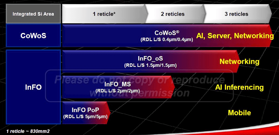
For CoWoS, Yu also stated:
- Over 50 customer products have shipped
- Up to five interconnect layers on silicon interposers are available, as well as deep-trench capacitors
- To date, the largest customer design combined 2 large logic die and 8 HBM2s on a 2460 mm2 interposer in a 75 x 75 mm package
For InFO, Yu reported progress like:
- An InFO_oS (on-substrate) design combined nine dice with 130 mm bump-pitch
- In 2020 40 mm bump-pitch will be supported
- The InFO_MS qualification, with an HBM2, will be completed in 2H’19.
Yu also mentioned a project where they combined 49 dice, in a 7×7 matrix, on a thermal module base. (Remember Synergy’s wafer-level integration plans in the ‘80s. Will TSMC break down another sound barrier?)
TSMC also offers wafer-to-wafer bonding, down to 2mm pitch and die-to-wafer bonding at >9 mm pitch with 4 mm diameter TSVs.
The Importance of Design-enablement
Full disclosure: My key reason for leaving National Semiconductor and later VLSI Technology was the lack of management support for IC design enablement tools. I joined ViewLogic, a design tools vendor, in 1987. My first customer visit was to TSMC. When Synopsys acquired ViewLogic, less than a year later, my team at Synopsys and Dr. Cliff Hou’s team at TSMC, developed the first reference design flows and PDKs, to differentiate TSMC’s capabilities from their many contenders.
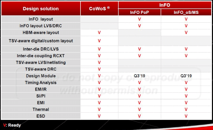
Since that time, TSMC always paid a lot of attention to enhancing their Design Enablement capabilities. They won big in the fabless and foundry business. Yu confirmed with Figure 3 that TSMC’s Design Enablement capabilities for IC packages follow this successful tradition. It outlines hows how many physical, thermal and electrical constraints a package designer needs to manage, to achieve a reliable and cost-effective solution. With the increasing complexity of multi-die designs, all these analysis/verification steps will get even more demanding — and unsolvable without the right design enablement support.
Special thanks to Dr. Cliff Hou and his team for supporting Yu’s engineers with the right design capabilities!
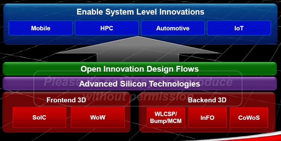
Yu’s closing slide, Figure 4, shows that TSMC is well positioned to meet these requirements and enable customer innovations. It also reminds us that TSMC clearly leads the path to higher-level and higher value system-level building blocks. The many open Innovation Partners TSMC invited to exhibit at this event, reminded everybody that no company can succeed on its own. Ecosystem-wide cooperation is essential for success in our demanding industry.
Thank you for reading this blog. At this point I hope you’ll understand why I am pushing in my blogs and presentations – sometimes too aggressively – for ecosystem-wide cooperation, and emphasize the importance of EDA design tools. ~ Herb


