
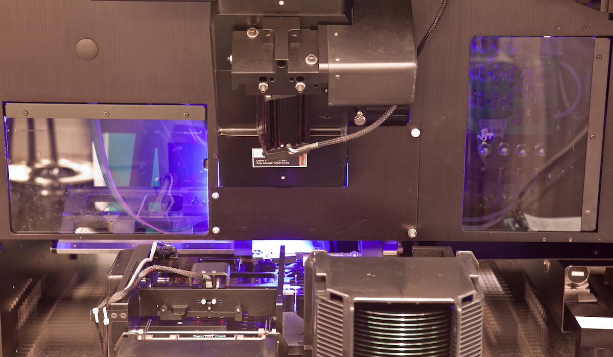
 Materials have a major impact on reliability, performance, cost and other key parameters of electronic solutions. SEMI’s recent Strategic Materials Conference (SMC 2019) brought materials suppliers and their customers together to discuss progress made in these areas. They also addressed how to solve the increasingly divergent and complex challenges current and future applications have in store for the semiconductor industry. In addition to the keynotes, the conference sessions focused on business trends, substrates, More-than-Moore, emerging materials, automotive requirements, and fabs.
Economic and Market Trends: The Big Picture
Predicting the future is difficult, especially in today’s very dynamic market conditions. It’s very challenging for executives to plan and invest and they prefer to err on the “save” side – which means spending less. Duncan Meldrum from Hilltop Economics and Len Jelinek from IHS Markit explained some of the challenges created by our 10+ years old expansion combined with a shaken-up supply chain and provided some guidance to attendees of the Strategic Materials Conference.
According to Meldrum, semiconductors are a major industry factor today. According to Meldrum, semiconductors are a major industry factor today. They impact 15% to global GDP, compared with 5% in 1990. He also said that the aggregate profit margins of US companies have fallen from 13 to 10% in the last two years, which is leading to decreased investment. On the other side, full employment allows consumers, who are controlling 70% of our economy, to continue spending. However, early warning signs, like less spending in restaurants, is a recent indicator of a possible decline in consumer spending.
Meldrum doesn’t expect a shock to our economy. He predicted a slight reduction in growth rate, starting in 2020 or ‘21. Jenilek noted that increasing memory prices and 5G technology for handsets and other applications will bring new revenue opportunities. At the same time, he warned that the cyclical nature of the semiconductors industry will remain. Both researchers agreed that markets and regions we are serving will react differently to a possible downturn. Therefore companies should monitor trends and opportunities in their customer base closely, and react to specific segments.
The speakers from Wall Street — Duffy Fisher from Barclays, and Krish Sankar from Cowen and Company — confirmed most of the market researchers’ observations, predicted more consolidation and warned that the bond market signals concerns. They praised business models that guarantee recurring revenues, like the software industry’s time-based licenses (TBLs), because they secure constant revenue streams for several years ahead. Both financial analysts conveyed that investors expect semiconductors, especially materials, to become more important for serving electronic systems and the global economy. This sentiment should attract more investments, notwithstanding the long payback periods in our industry.
Weaker stock market performance, lower than expected manufacturing and services numbers and declining 10-year bond rates during the week after SMC 2019, lent further credibility to the experts mentioned above.
Strategic Materials Conference Keynotes from Ford, TSMC and Entegris
The keynotes from three very different companies spanned the entire supply chain and highlighted dependencies.
Dragos Maciuca, from Ford’s Palo Alto R&D center, started his keynote by showing how rapidly the San Francisco Bay Area has been attracting R&D centers of automotive companies and their suppliers. He walked us briefly through the levels of car autonomy: Hands-on – hands-off – eyes off – mind off – driver off (= full autonomy). Maciuca also explained trade-offs between radar, lidar and camera fusion and the importance of internet connectivity. He predicted that electrical power trains will replace internal combustion engines (ICEs) within the next few decades.
Maciuca questioned today’s car ownership model, where cars are parked 90% of the time. It may not be sustainable and lead to a decline in car sales. The automotive industry is also concerned about the many business and legal hurdles fully autonomous vehicles may have to surmount. Ford is hopeful that the 70 start-ups currently working on Lidar systems can bring the unit cost down to about $200 to enable mass deployment of this highly accurate sensor technology. It can help to reduce the number and severity of accidents. He left no doubt that electric power trains and self-driving (level 3 to 4) will become very important and widely accepted but warned not to believe all the hype about instant progress to fully autonomously driving passenger cars. However, less cost-sensitive vehicles, like trucks, will soon be fully autonomous, exclusively for highway driving.
The second keynoter, Carlos H. Diaz, Senior Director, Corporate Research, TSMC, conveyed a very encouraging top-level view of my favorite subject: System-level integration using multi-die ICs. He emphasized that TSMC’s business stands on three very strong pillars:
- CMOS advanced technology, e.g. N7, N6, N5,
- Specialty technology, e.g. RF, BCD, Sensors, and
- 3DIC technology, e.g. SoIC, WLCSP, CoWoS.
While today the largest ICs contain up to 50 billion transistors, Diaz expects TSMC to make up to 200 billion possible using 3DIC technology. After having relied on immersion and multi-patterning, TSMC is now utilizing also extreme ultra-violet (EUV) technology and expects to deploy directed self-assembly (DSA) as the next step. Diaz emphasized the need for new materials to reduce contact resistance and voltage drop, as well as to improve electron/hole mobility on the die. He also mentioned the need for highly parallel architectures – e.g. combining CPU and high-bandwidth memory (HBM) on an interposer, utilizing thousands of interconnects. Last, but not least, Diaz indicated that TSMC recognizes the need for a memory alliance.
The third keynote, titled “Chemical Companies at a Crossroad” was presented by Bertrand Loy, President, and CEO of Entegris and Vice Chairman of SEMI. He expects an industry downturn and highlighted that SEMI’s MSI report, tracking Millions of Square Inches of wafers shipped, is an early indicator of industry trends. Loy suggested a number of steps companies should take to better prepare for future challenges, such as the demand for faster, cheaper, and more reliable ICs. To meet these requirements, Loy recommended focusing on contamination control at every manufacturing step and introducing the latest metrology capabilities. Loy referred to the very high-margin pharma industry as an example of the benefits of high R&D spending to create innovative and high-value products.

More about Heterogeneous Integration at the Strategic Materials Conference
Our 3D InCites readers will like to hear that TSMC was not the only big supplier talking about heterogeneous integration during the Strategic Materials Conference.
Representing Intel, Sairam Agraharam, a Georgia Tech graduate, explained Intel’s solutions for multi-die ICs. He explained the Embedded Interconnect Bridge (EMIB) for connecting side-by-side dice with silicon strips, embedded in organic substrates, Intel’s recently introduced Foveros 3D vertical stacking solution and their CoEMIB technology, which allows assembling dice in both horizontal and vertical directions.
John Hunt, Senior Director Engineering and Technical Promotions at ASE, the world’s largest IC packaging house, started his presentation about fan-out packaging with a very telling comparison: Apple’s iPhone 1 used one wafer-level package (WLP), the iPhone 10 contains 72. They minimize iPhone size, especially thickness, reduce board space needed, device power and weight while increasing performance. Hunt showed the many development steps ASE’s engineering teams had taken, to achieve the impressive progress in IC packaging.

Summary
Many other presentations and discussions focused on wafer manufacturing topics – clearly today’s largest opportunity for materials suppliers. Some presenters and especially the panelist in Session 7 emphasized that suppliers of simple commodity products will suffer most if/when a downturn comes and encouraged the audience to expand their domain expertise for serving target markets with differentiated and high-value (sub)system-level solutions.
Since 1998 I have observed how much impact the cooperation between wafer manufacturers and EDA vendors has on the semiconductor industry, especially the growing number of fabless IC vendors. Jointly developed process design kits (PDKs) and die reference design flows for every new node accelerate its market acceptance, drive innovation, revenues and profits. 20+ years after this successful fabless and foundry business model started, we have now the opportunity to extend Moore’s Law with advanced packaging technologies, to serve the increasing demand for heterogeneous integration.
Now IC package manufacturers (OSATs) and EDA vendors need to cooperate, to jointly develop package assembly design kits (PADKs) and package reference design flows for widely used IC packages, especially when containing multiple dice, to accelerate their market acceptance. Similar to the fabless & foundry cooperation, the OSAT, and EDA cooperation will also bring significant productivity gains in package design and manufacturing, reduce the costly margins needed today, increase device reliability and enable much higher complexities, performance and profit margins.
I am hoping SMC 2020 will offer OSATs and their EDA partners opportunities to share their experience with PADKs and package reference design flows.
Thanks for reading…Herb


