
Key advanced packaging technology influencers came out in force to discuss the status of EDA tools for 2.5D/3D IC package design at the recent User to User (U2U 2019) Conference, organized by Mentor, A Siemens’ Business (Mentor) and hosted at the Santa Clara Marriott. Presenters from Wave Computing, ARM, Amkor, TechSearch International Inc., and Qualcomm lent their voices to the cause.
Technology Trends
In his keynote that kicked off the general session, Joe Sawicki, Executive Vice President, and product line manager at Mentor, talked about technology trends and how Mentor has positioned itself to provide solutions that span the supply chain. (See feature photo.)
Sawicki reminded everybody that in Fall 2016, when Siemens acquired Mentor Graphics, there were many skeptical and doubtful voices commenting on this combination of industrial prowess and electronic design software tools. In the meantime, Siemens acquired three more EDA companies and grew their R&D investments in this space by 25%. “Digital Twin” became a household word and most of the previous skeptics and doubters have been converted, as Mentor, beats even optimistic expectations.
Emphasizing that ASML is delivering on the promises of EUV and enables further feature size shrinking, Sawicki confirmed that Mentor completed its contributions to 5nm nodes and is now working on 3nm technology nodes.
Sawicki agreed that energy density and the exploding number of design rules represent significant challenges, but he expects that higher levels of abstraction, domain-specific architectures, machine learning (ML), moving more computing tasks to the Internet of Things (IoT) edge-nodes and other technology trends will enable semiconductor and electronic systems experts to continue innovating.
Allen Sansano, VP of Engineering at Wave Computing and Vicki Mitchel, VP Technology Services Group at ARM, also spoke during the general session, describing their priorities and cooperation with Mentor, in the general session too.
HDAP Market Update
The conference offered nine break-out sessions. Of course, “Xpedition, High-Density Advanced Packaging (HDAP)” was my choice. Keith Felton, Product Marketing Manager at Mentor, managed the session and introduced the presenters, all experienced EDA and/or packaging experts. They conveyed a broad range of important topics, from a big picture market research overview to detailed technical essentials, like extraction.
Jan Vardaman, President at TechSearch International, gave an HDAP market update and addressed in her presentation many questions in HDAP users’ minds.
Figure 1 shows major packaging alternatives and several selection criteria to narrow down the many choices.
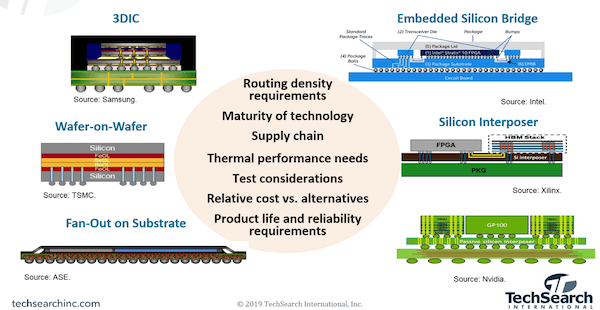
Vardaman highlighted that multi-die advanced packages enable not only cost-effective integration of heterogeneous functions but also allow the implementation of new architectures to further increase performance per Watt. She showed many examples for successful 2.5/3D-IC designs and outlined a growing list of major suppliers: GlobalFoundries, TSMC, and UMC manufacture silicon interposers; Ibiden, Kyocera, Semco, Shinko, and Unimicron offer organic interposers. Vardaman also mentioned that Micron will introduce their HBMs in 2020. To confirm the importance of HDAP technology, she stated that TSMC’s back-end revenue was $ 2.5 billion in 2018.
PDKS vs. PADKs
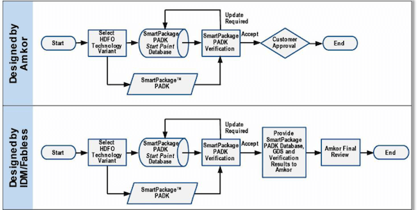
The next guest speaker was Ruben Fuentes, VP worldwide design, Amkor. He started out with comparing process design kits (PDKs) from wafer foundries, which are relatively static these days, to package assembly design kits (PADKs), which are very new today and need to be flexible, as customer requirements and technology capabilities keep changing rapidly.
Amkor chose to develop their first PDAK to support their wafer-level packaging technology, silicon wafer integrated fanout technology (SWIFT™). Fuentes emphasized that this PADK not only contains design rules but is also linked to Amkor’s computer automated manufacturing (CAM) system to avoid surprises during production ramp-up. This PADK outputs GDSII format because the traditionally used Gerber format can no longer manage the complexities of new SWIFT designs. Figure 2 shows how Amkor’s PADKs support high-density fan-out (HDFO) turnkey designs for customers and joint designs with development partners.

Fuentes summarized his talk by emphasizing that without PADKs and die-package design tools, the complex designs customers require today can be no longer managed.
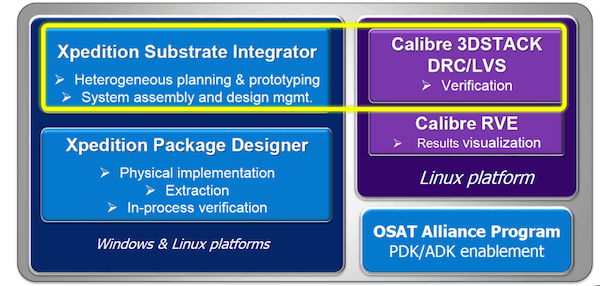
Another guest speaker was Magesh Govindarajan, Senior Staff Engineer at Qualcomm. He is a power user of Mentor’s package design tools – Xpedition Integrator for design planning and implementation as well as Calibre 3D Stack for DRC & LVS verification and design sign-off. Govindarajan outlined the benefits of having design kits and design tools support to enable die-package co-design. He mentioned that Qualcomm insists now that all their IC packaging partners provide design kits.
Design Tools and Methodologies
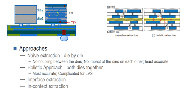
These three guest presentations set the stage for tools and methodology experts from Mentor to convey their strengths. Dusan Petranovic, interconnect modeling Technologist, outlined his role and explained why accurate parasitic extraction is very important for timing analysis and for assessing the effects of coupling between through silicon vias (TSVs), between Re-Distribution Layers (RDLs) and also between TSVs and RDLs. Especially complex and critical is assessing coupling effects, if dice are stacked vertically and face-to-face. Figure 3 shows how capacitive coupling in such a configuration impacts both circuits and lists different extraction strategies.

Chris Cone, technical marketing engineer, Mentor, summarized the session’s presentations with market data, individual design tool highlights, and explained their place in the complete design solution (Figure 4).
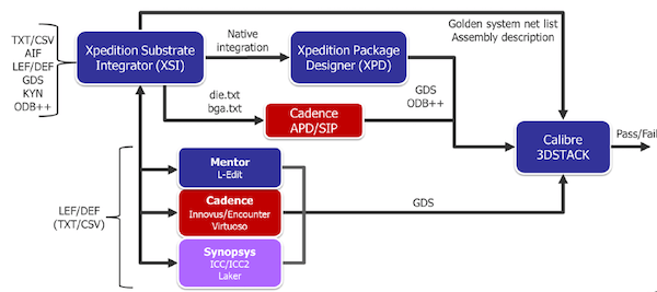
Because many customers use and trust tools from different suppliers, Cone also showed which data formats and multi-die design flow utilizes and how other vendors’ tools can interact within a Mentor flow (Figure 5).
2.5D/3D IC Design: The Obvious Choice
In May 2008, during one of my Global Semiconductor Alliance (GSA) working group meetings, we decided to emphasize the development of EDA tools for 3D-ICs. All EDA experts in the room agreed that using the third dimension will increase IC and system performance significantly while saving power, board space, and cost.
Exactly eleven years later, the presenters, as well as the audience of the “Xpedition, High-Density Advanced Packaging” session realized that we, as an industry, decided wisely to choose this path and execute. Of course, there is still a lot of technical and business development work to be done, like more user-friendly die – package – board design methodologies, a comprehensive library of die-level building blocks (a.k.a. chiplets), accurate models for these chiplets at different abstraction levels, new IC packaging materials and manufacturing flows, clear win-win business models and other efforts. They’ll make 2.5/3D-IC technology an obvious choice, like following Moore’s Law did for the last fifty years.
Looking forward to meeting you again at the Advanced System in Package Conference in Monterey, June 25 to 27, at ES Design West and Semicon West, co-located in San Francisco, July 9 to 11.
Thanks for following this blog ~ Herb


