 More than 20 years ago, the cooperation between fabless IC vendors and wafer foundries started to dominate over the integrated device manufacturing (IDM) business model and established clear interfaces between design and manufacturing companies. Ever since IC designers can only create a single-die system-on-chip (SoC) design if a process design kit (PDK) informs them about their wafer foundry partner’s capabilities and limits.
In recent years, the technical and cost constraints of single-die SoCs encouraged industry leaders to implement their ideas in multi-die system-in-package (SiP) designs. This has shifted a lot of the value creation from dice to the package. It’s only logical that SiP designers are now asking their outsourced semiconductor assembly and test (OSATs) partners for a package assembly design kit (PADK), that specifies their partner’s capabilities and limits.
Packages comprise interposer(s), vias, micro-balls, substrates, over-mold, and more. These use different materials with widely diverging electrical, thermal and mechanical characteristics. Understanding how these materials interact during the manufacturing process and during real-life operation is very critical for SiPs’ yields, performance, and reliability.
Thus the title of this year’s SEMI’s Strategic Materials Conference (SMC 2019): A Year of Transition, Material Opportunities, and Challenges.
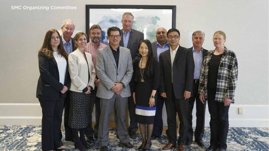
SMC 2019 takes place at the DoubleTree Hotel in San Jose, from Sept 23 to 25, 2019. It brings materials suppliers and users together to address these topics and assure cost-effective design and manufacturing of reliable single and multi-die ICs. Learn more about it here.
This year for the first time the SMC is brought to you by SEMI’s recently formed Electronic Materials Group. This new collaborative technology community that combines the former Chemical & Gas Manufacturers Group (CGMG), the Silicon Manufacturers Group (SMG) and other SEMI member segments to better serve the interests of the $69 billion electronics materials industry. The group is open to SEMI members involved in materials manufacture, distribution, and services throughout the microelectronics industry. ~ Herb


