

 The Microelectronics Packaging & Test Engineering Council (MEPTEC) held its monthly meeting at SEMI in Milpitas on April 10. Two speakers outlined their companies’ capabilities and demonstrated their own expertise in solving specific industry challenges.
Tom Gregorich presented why and how Zeiss supports IC package inspection with 3D X-ray machines, then Sitaram Arkalgud conveyed the benefits of Xperi’s direct bond interconnect (DBI™) technology for interposer (2.5D) designs and vertical die stacking (3D).
The Magic of 3D Xray
Zeiss, headquartered in Germany, is well known as a supplier of microscopes, camera lenses, and binoculars. They can do more. Gregorich titled his message “Measurement of Buried Features in Packages Using 3D X-ray”. He started with a brief look back in time and explained that inspection of package defects traditionally relied on the sharp eyes and skills of human operators, only supported by magnifying lenses. In recent years increasing pin-count, multi-die assemblies, higher signaling speeds, higher power, and other parameters have made IC packaging much more complex and shifted a significant part of ICs’ value creation from the die to the package.
Avoiding hidden cost in the package assembly process — e.g. caused by poor yields and quality problems or missed market windows and lost opportunities — is becoming more important. More thorough and more sophisticated inspection procedures are now clearly needed and economically justifiable.
Because IC final tests only check for electrical performance to be within specific margins, they rarely detect marginal mechanical dimensions inside a package that may lead to reliability problems. This can result in expensive field failures and makes the benefits of 3D X-ray package inspection much more compelling. Gregorich showed how Zeiss applies its metrology expertise to the growing number of IC package inspection challenges. Figure 1 shows a number of defects their Versa 3D X-ray system can detect and visualize.

Figure 2 shows how these 3D X-ray systems accomplish the tasks of capturing, tracking, computing and clearly visualizing defects on prototypes during manufacturing flow development and/or failure analysis. Likewise, in-line inspections allow QA experts to monitor manufacturing margins on samples and, if necessary, fine-tune the manufacturing flow to assure highest yields and best quality products.

The four quadrants in figure 2 show:
- how parts are loaded onto rotating carriers to offer the X-ray beam a 3D perspective,
- How the inspection station reconstructs the acquired 3D data and passes it on to
- The manufacturer’s host computer for data storage and analysis.)
- Indicates that Zeiss equipment, in addition to visualizing defects and manufacturing margins, uses 3rd party software to analyze repetitive measurements and generate production reports.
In response to a question from the audience, Gregorich explained that Zeiss’ business model is to focus on supplying the equipment for 3D X-ray inspections. If customers are interested in 3D X-ray inspection services, Zeiss refers them to 3rd parties.
Die-to-Wafer Hybrid Bonding is Here
In the second half of this luncheon, Xperi’s Sitaram Arkalgud briefly explained the ZiBond process – Oxide to Oxide bonding – then the DBI process and its applications for wafer-to-wafer (W2W) stacking, as shown in Figure 3. He emphasized that Xperi has also developed a die-to-wafer (D2W) process flow to enable the bonding of different size dice.
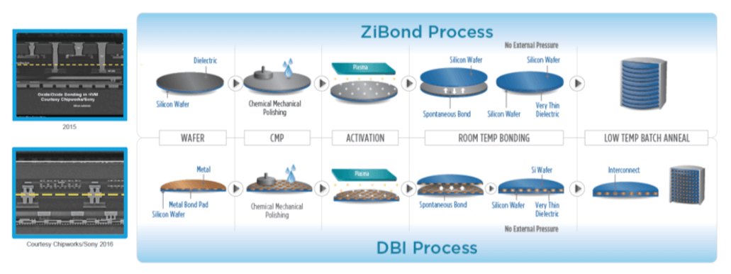
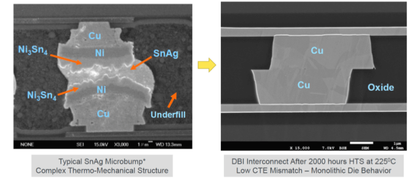
Using a face-to-face example, Figure 4 shows how the mechanically strong and low resistance connections are accomplished. Key point: Copper (Cu) expands significantly more per °C than oxide, and creates a mechanically strong bond and a very good electrical contact without external pressure at relatively low temperatures. Arkalgud emphasized that these process steps need to be performed in a cleaner environment than typically used for package assembly. Having said this, he stated that Xperi achieves yields in the high 90s in their Class 1000 cleanroom.

Compared to the complex chemistry in today’s microbumps, DBI connections simplify the manufacturing process flow, eliminate the need for underfilling, reduce Z-height, as well as significantly enhance thermal connectivity and vertical heat-flow. In addition, the much smaller DBI contacts, versus microbumps or Cu studs, reduce interconnect capacitance (C) and path inductance (L). Last but not least, the direct Cu-Cu connections offer much less resistance (R) than above-mentioned methods and, with all these RLC advantages, increase circuit performance while reducing heat generation at these vertical interconnects. Figure 6 compares cross sections of both interconnect technologies.
Just in case all these benefits were not convincing enough, Arkalgud added that the DBI density of 100k to 1 million connections per square mm, exceeds micro balls’ interconnect density by several orders of magnitude.
Considering the rapidly growing and very demanding opportunities for semiconductors in an automotive application, Arkalgud also showed DBI qualification test results that exceed requirements (Figure 6).

Arkalgud reported that DBI for W2W stacking has been in high volume production for years in CMOS image sensors, used in RF applications, and is gaining ground for stacking memories.
As D2W placement equipment now offers high throughput at < 1-micron placement accuracy, the DBI benefits can also be utilized economically for D2W manufacturing.

In response to a question from the audience about the testability of vertically stacked dice, Arkalgud showed an Xperi test vehicle, where the top die was smaller so that the test pads on the periphery of the bottom gave access to the entire circuit. People can also use thinned top dice and open probe pads that connect to the top or bottom die – it depends.
In response to my question, Arkalgud confirmed that DBI and the die placement accuracy available now, also lend themselves perfectly for placing chiplets onto interposers. This will make 2.5D designs and the use of chiplets even more attractive.
DBI Q&A
During the Q&A several more topics were raised and answered by Arkalgud:
Q: Is DBI limited to face-to-face stacking?
A: No, TSVs enable DBI for face-to-back or back to back stacking.
Q: What about stacking more than two dice?
A: TSVs also enable multiple dice to be stacked, as Arkalgud showed a slide with 20 dice, each 50µm thick, stacked – at a total height of only 1 mm.
Q: How can a user avoid large TSVs, that would counter DBIs tight interconnect density?
A: Stacking additional wafers on the (thicker) bottom wafer allows thinning of the upper wafers, down to 10 microns, and enables TSVs down to 1µm diameter.
Looking forward to meeting you at future MEPTEC luncheons. For schedules and agendas, please check here. Thanks for reading these two presentation summaries….Herb
Editor’s Note: Featured image depicts the visualization of C4 bumps, TSVs, and Cu pillar micro bumps in a 2.5D package using Zeiss Versa 3D X-ray system, courtesy of Zeiss website.


