
 In addition to Francoise’s post about technology megatrends here, below is part one of my perspective, mostly about the SEMICON West keynotes.
Design and Manufacturing Are Finally Combining
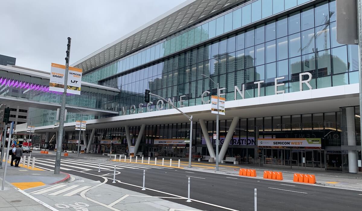
From July 9-11, many IC manufacturing experts came together at SEMICON West in San Francisco’s very nicely renovated Moscone Center. As an industry first, a small number of Electronic Design Automation (EDA) experts, presented Electronic System Design (ES Design) West and shared space in the South Hall with manufacturers. Next year, I hear, the EDA industry’s traditional Design Automation Conference (DAC) and Semicon West will be co-located at the Moscone Center. This will offer many more “one-stop shopping” opportunities for our mutual customers.
Key Applications and Major Technology Trends
It’s great to hear that funding for artificial intelligence (AI) and machine learning (ML) developments is increasing significantly, however, some realism about remaining AI challenges and capability limits is recognizable. AI guru Kai Fu Lee’s interview on CBS’ 60 Minutes, is an impressive summary of these and other AI topics.
Regarding 5G, deployment of the sub 6GHz variant is progressing well. However, people realize that the many micro-cells needed to offer the additional benefits of the mmWave portion of 5G technology widely will take some more time and investments.
In the discussion about the future of Moore’s Law and the need for More than Moore, I got the impression that some Moore’s Law supporters feel that they need to defend their turf against a More than Moore take-over. Based on my decades of experience with following Moore’s Law and now focusing on More than Moore, I can assure you that technology transitions were not and won’t be zero-sum games. The rapid growth of More than Moore designs as system-level solutions will actually broaden the market opportunities for Moore’s Law designs significantly — if not as fully packaged devices, then as space and power-saving die-level building blocks (a.k.a. chiplets). In my next SEMICON West blog I’ll report about the progress wafer-probe and architecture experts are making to enable high-quality chiplets and suitable interconnects for reliable system solutions.
SEMICON West Keynotes from C-level Executives
On Tuesday, a series of impressive keynotes drew many people to the Blue Shield of California Theater, right next to the North Hall. Dave Anderson, President SEMI Americas, welcomed the audience and gave an encouraging industry overview. He pointed out that a large amount of data, generated by billions of IoT edge-nodes and the rapidly emerging AI capabilities, will contribute to continuing our industry’ growth.
Aart de Geus, Chairman and Co-CEO, Synopsys, assured us that Moore’s Law will continue to play an important role. He emphasized the contributions of electronic design automation (EDA) tools for improving system security and delivering better and cheaper products sooner to our customers. He reminded us that the vertical markets we serve have very different and quite challenging requirements, that are best served by co-optimizing customer-specific solutions in cooperation with other companies across the entire supply chain.
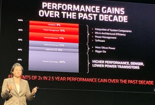
Lisa Su, AMD’s President and CEO stated that her company’s focus is to deliver high-performance computing (HPC) solutions at lower power. She explained that the I/Os consume about 30% of a single-die SoC’s power. In comparison, only 33% of the IC’s total power is utilized for computation. Su suggested a three-prong approach:
- Changing the microarchitecture using AMD’s Zen 2 architecture
- Utilizing chiplets and die-stacking, for example, EPYC chips that combine 4 dies with 8 cores each on an interposer
- Heterogeneous platforms to improve performance per Watt, such as with AMD’s CPU + GPU + FPGA platform
Su closed by proudly announcing that the “Frontier” super-computer at Oak Ridge Labs uses AMD CPUs and GPUs. Figure 1 shows Su explaining that about 50% of performance gains came from silicon-related innovations, 17% from a better microarchitecture, 15% from smarter power management and 8% of the performance gains during the past decade were contributed by compilers.
Gary Dickerson, President and CEO, Applied Materials, explained that not only the speed of AI innovation, but also society’s acceptance, security and safety as well as sustainability considerations will determine when AI will be adopted widely. He compared today’s general-purpose computing with AI-based computing (Figure 2).

Dickerson confirmed that more of the computing tasks are moving to the edge because otherwise, the installed communications equipment won’t be able to keep up with the flood of data 500 Billion IoT devices will want to send to the compute centers in 2030. He stated that Moore’s Law is “running out of gas” and added that new architectures and structures (example: 3D NAND) are clearly needed. New materials – for the die and IC packages – and advanced packaging technologies are already enabling new ways to shrink systems and saving power while increasing performance.
After a brief lunch break, several relatively technical presentations followed.

A Look to the Future
Cliff Young, an engineer from Google, started his message with several impressive statements: A Tensor Processing Unit (TPU) offers 10x improvement in the total cost of ownership (CoO) and offers 15 to 20 times the performance per watt, compared to a traditional CPU. He also talked about the benefits of co-design, inter / multi-disciplinary work, two-dimensional pipelines (a.k.a. Systolic Arrays) and explained why trading off precision for reducing die area, cost and processing time makes sense. He closed with telling us that deep learning (DL) needs more than Moore’s Law to succeed widely, such as analog and/or optical computing, better non-volatile memories, in-memory processing, 3D structures, quantum computing, storage devices for optical signal and a way to manage signal-to-noise ratio in analog computers. … Lots of ways to put Google’s R&D money to good use.
Jeff Bier, Founder Embedded Vision Alliance and President BDTI, talked about perceptual algorithms and the progress they are making in image recognition — including face recognition. He thanked the many VC funds that invest in this, “previously virtually impossible” domain.
Renee St. Armant, Research Engineer in Emerging Technologies and U.S. Innovator of the Year, works at ARM. She also believes that Moore’s Law is outdated and emphasized that what really counts is the value of technology for society, such as simultaneous translation utilities and behavioral processing units (BPUs) that recognize fatigue, fear, and other human behaviors. Also, edge computing (a.k.a. in-situ computing) is valuable, because it reduces latency, bandwidth requirements as well as improves privacy and security. She closed with predicting that ML will open the door to many new vectors of innovation.
Today’s Hot Topics
After the previous three presenters looked primarily far into the future, Chidi Chidambaram, VP Process Technology and Foundry Engineering, Qualcomm, stayed closer to today’s hot topics AI, ML, and 5G. He confirmed the importance of edge computing and AI with a very telling example: Instead of streaming all its data to the cloud, a security camera should be able to decide which two minutes – out of a 24-hour day – are relevant to be transmitted to the cloud for safe-keeping or immediate use.
Chidambaram talked about the differences between the sub 6GHz band and the mm-wave part of the 5G technology and Qualcomm’s Snapdragon 855, which supports both. Qualcomm sees MRAMs as high-potential technology and realizes the need for further power saving, e.g. by reducing precision, computing in memory and/or by using quantized accelerators for 24 / 8 / 1 bit. To illustrate the challenges of wireless communication, he stated that a power amplifier needs to send 20dB signal, while a receiver needs to capture -100dB signals securely.
The keynotes as well as the other sessions I was able to attend, were all very well organized and rich in content. They showed that the semiconductor industry is committed and ready to continue our high-growth path, even as memory prices, political uncertainties and lots of new requirements raise the bar. When capturing the feedback from many EDA exhibitors, I learned a lot. I look forward to assist combining Manufacturing and Design experts in July 2020 even more effectively.
In my second SEMICON West blog, next week, I’ll report about the HIR meetings I was able to attend, the imec Technology Forum and the very impressive Test Vision Symposium. Thanks for reading …… Herb


