


SORIN CRM: 3D IC Module for Active Medical Implant
Manufacturing of 3D IC heterogeneous integrated modules for the electronics of a leadless pacemaker in a very small volume has been realized. Manufacturing of 3D IC modules using the described process is ready for medium volume production. Testimonial All the electronics of a leadless pacemaker has been integrated into a...
SETNA: Process for Room Temperature 3D IC Assembly
SETNA, in conjunction with Research Triangle Institute (RTI), has developed a binary alloy (Silver-to-Indium) bonding system for 3D IC assembly that can be compression-bonded at room temperature. Following 3D IC chip stacking, the Ag-In structure is annealed in the solid-state (no melting) to form an Ag₂In interconnect which is stable...
Schiltron 3D Flash
Schiltron 3D Flash replaces 2D-NAND. It uses a unique architecture solving key challenges associated with other 3D-NAND approaches: scalable; no vanishing string currents; uses existing Fab infrastructure and materials; uses existing design approaches for program and erase; endurance of over a million cycles; post-cycling retention of more than 10 years...

3D InCites Interview: RTI in 3D
While most of the research institutes in the US and Asia have been focused on commercializing 3D integration technologies for mass markets such as mobile devices and consumer electronics, one US-based research institute has followed a different path more similar to that of the European research centers; focusing its 3D...

Are Design Tools and Thermal Solutions the Missing Links to 2.5D and 3D IC Production?
On one side of the fence, we have semiconductor device manufacturers (fabs, foundries, and OSATS) claiming to be ready to ramp 2.5D and 3D IC devices to production, saying that remaining issues can be engineered out. On the other side, we have system integrators who, while they believe 2.5D and...

Should EDA vendors, OSATS, and their customers cooperate more?
Last week, I attended the packaging-focused 64th Electronic Components and Technology Conference (ECTC) 2014 in Orlando. This week I spent three days at the EDA-focused 51st Design Automation Conference in San Francisco. In addition to realizing that these two locations are about three thousand miles apart, I noticed that the...
SPTS: Blanket Silicon Etch Process for Via Reveal
The blanket silicon etch process performed on the SPTS Rapier XE achieves an etch rate >8.5µm/min, high selectivity (Si:SiO>150:1), and is ~3-4x faster than competing systems. A unique dual plasma source design creates a uniform etch (<±3%) across a 300mm wafer, which can be “tuned” to compensate for variations in in-coming...
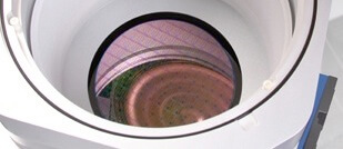
Novati Technologies: Silicon Interposer Module
The 2.5D Interposer Module features three front-side interconnect layers of dual-damascene copper on top of a single-damascene copper metal layer, with 2µm Line/Space/Thickness interconnect dimensions. The via-first TSVs are copper-filled with a 10:1 aspect ratio and via-last TSVs are copper-lined, polyimide-filled with a 5:1 aspect ratio, both with 50µm pitch....

Moore’s Law and More Than Moore Are Laws Of Economics: 3D IC At The 25th Annual SEMI ASMC
Saratoga Springs, NY, rolled out the red carpet the week of 19 May 2014 for the 320+ attendees, speakers, panelists, and journalists who participated in the 25th Annual SEMI Advanced Semiconductor Manufacturing Conference. Conference co-chairs Israel Ne’eman, Applied Material, and Oliver Patterson, IBM Microelectronics, presided over a group of talented...

Fine Tuning Processes for TSV Reveal
Through silicon via (TSV) reveal is a critical part of the wafer-thinning step in 3D IC backside processing, where the wafer is thinned to expose the Cu “nails” that ultimately form the interconnect between die stacks. Some of the risks involved in this step include backside contamination (Cu diffusion) due...
Setting the Record Straight On Applied Materials’ PVD Tool for 3D TSVs
Nothing makes me click a link faster than a title like “3D Chip Stack Tool Sends TSV Into High-Volume”, because who in this industry isn’t waiting for that precise moment when through silicon vias (TSVs) go into high volume manufacturing? Unfortunately, the EE Times story behind that provocative title was...

Glass Interposers Take the Stage at ECTC 2014
I have to admit, for some time I’ve been fairly skeptical about glass interposer technology as a viable alternative to silicon interposers. It’s not that I doubted the expertise of research scientists like Rao Tummala and Venky Sundaram at Georgia Tech’s 3D Packaging Research Center (PRC), who have been evangelizing about...

ECTC 2014: Bridging the Gap to 2.5D and 3D
Each year since I first attended the IEEE Electronic Component Technology Conference (ECTC) in 2009, the keynotes, panels and papers focused on 2.5D and 3D integration technologies has increased; every year, that is, until this year. At ECTC 2014, there were not any plenary or panels focused specifically on 2.5D...
E-System Design: Sphinx 3D Path Finder (“3DPF”) V3.0
The Sphinx 3D Path Finder (3DPF) is an exploration tool enabling fast test case creation and analysis for silicon and glass interposers containing: solder balls, pillars, bond wires, TSV/TSG as well as RDL interconnect structures. E-System Design: Sphinx 3D Path Finder (“3DPF”) V3.0 All based upon a patented simulation engine with the...
SSEC: WaferEtch TSV Revealer
SSEC’s WaferEtch™ TSV Revealer is a single wafer wet processing platform for 3D IC and interposer wet etching applications designed to reduce processing and capital equipment costs. The WaferEtch features superior uniformity of silicon thickness (as low as -/+ 0.7%). Testimonial Via reveal is a critical process step in 2.5D...

3D NAND Flash – Schiltron’s Answer
It probably appears that the only 3D technologies vying for 2D NAND’s crown are V-NAND from Samsung and p-BiCS from Toshiba/SanDisk, with their key selling point being their ability to use few lithography steps to build 3D stacked memory. For background, see Jim Handy’s series and mine. Here I will...
Lasertec: BGM300
The BGM300 was designed to enable quick and accurate measurement of Through Si Via (TSV) depths, Si wafer thickness, and Remaining Si Thickness (RST) above TSVs – all essential in a managed backside via reveal process flow. Back grinding errors due to “blind” grinding can lead to significant yield loss....
SSEC: Innovators in Single Wafer Wet Processing Tools
49 years ago, Solid State Equipment, LLC (SSEC) opened its doors with its first piece of semiconductor equipment; a seam sealer for welding the lid on hermetic packages. Today, that tool still exists, and although it now accounts for 1% of SSEC’s revenue instead of 50%, sales have remained constant...
Fogale: TMAP DUAL 3D 300 A
The TMAP DUAL 3D 300 A is a unique metrology and inspection tool available to the semiconductor industry capable of addressing all customer measurement requirements for MEMS and 3D packaging. The TMAP is highly flexible, accurate, and repeatable. The heart of this tool is based on multi-sensor heads which include...

News of 3D NAND Fab Construction: A sign of Progress or a PR Ruse?
While I don’t claim to be an expert in 3D NAND technologies, I do keep my eye on what’s happening in the 3D NAND market. So when two 3D NAND-related EE Times articles crossed my 3D radar in two days, I naturally checked it out. After reading both articles, I...