
Last week, I attended the packaging-focused 64th Electronic Components and Technology Conference (ECTC) 2014 in Orlando. This week I spent three days at the EDA-focused 51st Design Automation Conference in San Francisco. In addition to realizing that these two locations are about three thousand miles apart, I noticed that the packaging and EDA camps are still far apart in regards to share of mind for interposers and cooperation with each other in this field. Among the 1200 ECTC attendees and about 5000 DAC visitors, I noticed only a few who attended BOTH conferences and demonstrated interest in and knowledge about both camps. As more of the component value created moves from the silicon to the package, I suggest intensifying direct dialogs between EDA and OSATs instead of relying on silicon foundries as intermediaries.
In Orlando, Mentor Graphics was the only large EDA vendor exhibiting their package design tools. In addition, E-System Design, an EDA startup, demonstrated their path-finding tools for interposers and 2.5D designs. In San Francisco none of the large Outsourced Assembly- and Test houses (OSATS) exhibited and I met only a few packaging experts on the exhibition floor and/or in the sessions I attended.
I am not trying to question if the executives in both of these camps made the right decision regarding ECTC- and DAC attendance. I am certain they decided what’s best for their companies, based on the inputs the marketing- and business development teams provided. I want to encourage these teams at both EDA vendors and OSATs to analyze how their customers will compete in the market in 3 to 5 years discuss the importance of More-than-Moore solutions to win in their target markets.
Based on my recent observations, I expect that the very large semiconductor companies will clearly utilize 10nm and even 7nm FinFETs for their very high volume designs. These designs can recoup development cost in the hundreds of millions. But for medium- and lower volume designs most large and all smaller semiconductor vendors will need the technical benefits and modularity of interposer designs to lower NREs and shorten development times, even at the expense of initially higher unit cost.
Apropos higher unit cost: At ECTC several companies presented how they have lowered cost of 2.5D materials as well as assembly and test flows for interposer designs significantly – in parallel with improving production yield and device reliability. With detailed reliability studies several manufacturers conveyed that they are ready to ramp up volume production. However…
…During ECTC meals and in hall-way conversations several packaging experts told me that the number of 2.5D feasibility studies with customers is increasing further. But many of these customers don’t trigger volume production yet, because their current design flows and the fairly basic package design kits available don’t give them enough confidence that they can achieve optimal designs. Customers are asking for a closer cooperation between their system- and IC designers, IC packaging experts and especially IC design tools developers to help them walking the fine line between costly over-designs and unreliably under-designs.
A few highlights from ECTC’s 2.5D and 3D-IC focused sessions:
In session 1.3 Chaoqi Zhang from GeorgiaTech outlined this high-performance design using two large interposers. They developed, based on Oracle inputs, this solution for a complex computing application:
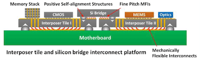
In session 19.4 Guilian Gao from Invensas presented this design with two 10×12 mm die (without TSVs) side-by-side and face-down mounted on an interposer. They are connected with more than 7000 microbumps at a 45μm pitch to this 120 μm thin 19×27 mm silicon interposer containing almost 8000 TSVs. C4 bumps connect this interposer to an organic substrate. Guilian outlined the manufacturing flow, discussed temperature profiles, showed SEM cross sections, answered detailed technical questions and conveyed that this kind of project is a routine challenge for her.

In the panel discussion on Wednesday evening Yasumitsu Orii from IBM presented a number of interesting data points: 1) In 2005 only 1% of the data traffic came from sensors, in 2020 experts project it to be 42%; a clear indication that the Internet of Things (IoT) will change our lives significantly. 2) IBM’s Watson, the computer that won against two Jeopardy champions, consumes 200 kW of power, a human brain only needs 20 W ⇒ Lots of room for improvement of our man-made storage- and computing systems. The ability of 2.5D/3D technology to significantly reducing form-factor and power dissipation will contribute to this goal.
The many 2.5D and 3D focused presentations and discussions at ECTC 2014 demonstrated that the IC manufacturing industry is exerting significant efforts not only to develop new capabilities, but also to lower cost and assure reliability of these technologies. As I projected at the beginning of this year: In 2014 interposer designs are ready, can be aimed and “fired” at a number of applications.
A few highlights from the 51st Design Automation Conference:
As indicated above, today’s 2.5D designers learned to live with limited EDA support and haven’t generated significant EDA revenues yet, therefore tools for this market did not get a lot of attention at DAC. FinFETs, double patterning, low-power design methodologies, higher levels of abstraction were much more important topics for presenters, exhibitors and visitors at DAC.
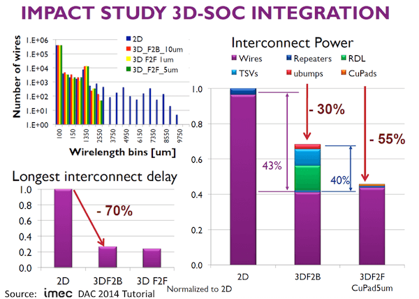
I had the opportunity to attend the 3D Tutorial and really enjoyed how BroadPak’s Farhang Yazdani and IMEC’s Pol Marchal explained 2.5D and 3D benefits for packaging- and silicon technology, respectively. Especially Pol’s slide below expresses very clearly how 2D SoC designs can benefit from 3D-ICs in regards to wire-length (= wire delay) and power dissipation from face-to-back and face-to-face vertical die stacking.
Because power-density and the resulting cooling challenges worry 2.5D and especially 3D-IC designers, I also found the fully depleted silicon-on-insulator (FD-SOI) presentation from STMicro’s Philippe Magarshack at the Samsung booth very useful. FD-SOI has none of the problems the old partially depleted SOI (PD-SOI) technology was plagued with (e.g. body effect, kink effect, high wafer cost…). FD-SOI also offers much better performance/power ratios and ultra-low voltage behavior versus bulk-CMOS as well as extremely low leakage. Planar 28nm FD-SOI transistors give you the performance of 20 nm bulk – without double patterning and allow back-biasing, unlike FinFETs. Dual-sourced (STMicro and Samsung) FD-SOI may also contribute to broaden market acceptance of 2.5D and 3D technology. ~ Herb Reiter


