
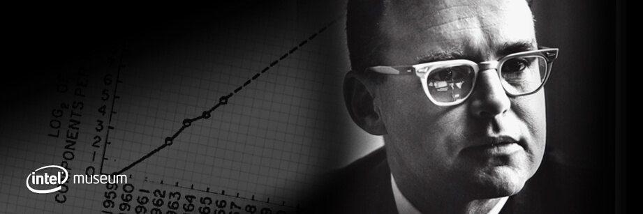

Saratoga Springs, NY, rolled out the red carpet the week of 19 May 2014 for the 320+ attendees, speakers, panelists, and journalists who participated in the 25th Annual SEMI Advanced Semiconductor Manufacturing Conference.
Conference co-chairs Israel Ne’eman, Applied Material, and Oliver Patterson, IBM Microelectronics, presided over a group of talented industry professionals from around the globe who joined together at ASMC 2014 for 3 days of networking, learning and knowledge-sharing on new and best-method semiconductor manufacturing practices and concepts.
 With one panel discussion, two tutorials (one on Silicon Photonics, and one on Directed Self Assembly), three keynote talks, and fifteen technical sessions on topics ranging from Advanced Process Control to Data and Yield Management to 3D / TSV Technology, along with an Interactive Poster Session, and a gala reception at Saratoga’s splendid Canfield Casino, there was a little something for everyone. If you haven’t attended one of the SEMI ASMCs in years past you should consider going in 2015. It’ll be well worth your time. (Full disclosure: I am an active member of the SEMI ASMC Steering Committee.)
Since we are looking back in time two weeks with this blog and interested mostly in the 3D IC perspective from ASMC 2014, I want to skip directly to the ASMC 2014 Day 2 Keynote talk on the “Innovation Pipeline for 10nm and Beyond,” presented by Dr. Mukesh V. Khare, Distinguished Engineer & Director, Semiconductor Technology Research, IBM Research at Albany NanoTech.
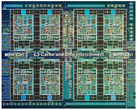 “Moore’s Law is a law of economics,” declared Dr. Khare, and, if the economics are right, it behooves manufacturers like IBM to manufacture massive (598mm², 2.75B transistors, operating at 5.5GHz) microprocessors built on SiGe technology for “Big Iron” computers. While making money in the process.
The semiconductor industry continues to find rewards in scaling ever smaller with traditional technologies but, sometime soon, the path beyond the 10nm process node will need to involve disruptive technologies. Dr. Khare offered silicon nanowires, carbon nanotubes, and III-V materials as being just three of the possible disruptive technology paths in development now for transistor fabrication in the era where we reach atomic scaling limits. But only if introducing those technologies makes economic sense. The market will choose winners.
And it’s the same for anything coming in on the More than Moore orthogonal: silicon photonics, Spintronics, and, yes, 3D stacking with TSVs, all have to make and win the economic case for their deployment before the industry will adopt them.
Maybe silicon transistor fabrication technology will reach an asymptote, maybe around the 7nm process node, where cheaper transistors just can’t be made anymore, and the industry falls off the Moore’s Law curve in favor of More Than Moore.
 The commercial aviation industry has already demonstrated a similar kind of end-stage maturity; once supersonic commercial aircraft had their (relatively) brief heyday the dominant players in the commercial aircraft industry chose to emphasize increases in fuel efficiency per passenger mile, and increases in flight duration (and better business class seats! And better entertainment options! On your 16 hour direct flight from EWR to HKG!), over choosing to invest in pure speed.
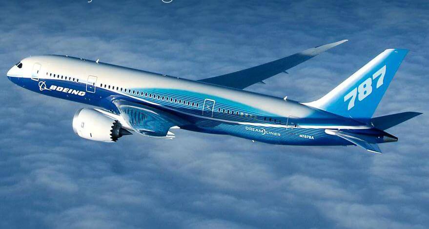
Is the sound barrier ceiling for commercial jet aircraft design something like the atomic dimension limit for commercial silicon transistor fabrication? When I asked Dr. Khare to consider that analogy in a follow-up conversation after his keynote he agreed that, yes, it is one way to think about things.
Meaning Dr. Khare’s 3D chip stacking—so long as the economics warrant—is going to be something like the composite construction; a super-efficient high-bypass turbofan engine generation of commercial aircraft on which we travel today. We won’t be traveling any faster with 3D chip stacking, necessarily, but we will be enjoying the advantages of the continued introduction of new technologies, and the performance improvements they bring.
There were six papers presented in the dedicated 3D / TSV Technology session at ASMC 2014, representing thinking from foundries and device makers (GLOBALFOUNDRIES, STMicro); academia (RPI, Tohoku University, CNSE); and a big-picture view from an analyst’s perspective (Yole Developpement).
I think Min Xu, CNSE, in her talk “RF Characterization of Through Silicon Via Test Structures in a 3-Tier Stacked Wafer,” captured the 3D IC zeitgeist with a single line from her talk: Xu and her colleagues, she said, fabricated the TSV test structures they studied in an “industry standard process line.”
Think about that for a moment. There’s a new generation of rising scientists and engineers for whom fabricating 3D TSV structures is an industry standard process performed in industry standard process lines.
GLOBALFOUNDRIES’ Fab 8 clean room in Malta, NY, a little down the road from Saratoga Springs, has just such an industry standard process line for via-middle TSV fabrication. For Sarasvathi Thangaraju, the important work now in achieving “Successful Void Free Gap Fill of 3μm, High AR Via Middle, Through Silicon Vias at Wafer Level” is about process fine tuning, not pathfinding. If you are an etch guy like me ,then Thangaraju’s reports on reducing “silicon spire” defectivity (root cause: bulk micro defects in the silicon wafer deliberately introduced as a getter layer) would have caught your eye, along with the work GLOBALFOUNDRIES has done to eliminate sidewall scallops in etched through silicon via structures.

We learned from M. Murugesan (who spoke on the subject of thin wafers and their mechanical properties relative to 3D IC processes at ASMC 2013) about the “Wafer Thinning for High-Density Three Dimensional Integration 12 Inch Wafer-Level 3D-LSI Program at GINTI.”
GINTI, the Global INTegration Initiative, is an 8”/12” R&D fab for the research and development of new 2.5D/3D integration technologies and creative applications. GINTI’s R&D fab is located in Miyagi Prefecture, Japan, and is about 15km from Sendai, which Tohoku University calls home.
Managing total thickness variation (TTV) across a thinned 12” wafer is a key deliverable in 3D IC process lines, and GINTI’s work has led to demonstrating <1µm wafer thickness variation across a 12” wafer with a final, thinned silicon thickness of 30µm. By using tiltable chucks during mechanical wafer thinning, by paying close attention to eliminating particles larger than 2µm during temporary wafer bonding, and by optimizing UV-assisted lift-off processes, GINTI reports they have an excellent handle on these critical 3D IC fabrication processes.
TTV was also an important consideration in the paper “Use of Optical Metrology Techniques for Uniformity Control of 3D Stacked ICs,” which was very capably presented by Delphine Le Cunff, STMicroelectronics. In order to control something you need to be able to first measure it; in STMicro’s case, three different optical metrology techniques (infrared interferometry, chromatic confocal, and multi-wavelength spectrometry) were used to measure TSV etch depths, carrier and carrier glue thicknesses on silicon wafers bonded to glass substrates, silicon wafer thicknesses during wafer thinning, and silicon wafer thicknesses during via reveal etching.
Some conclusions: TTV is governed by the glass carrier shape for a given TSV depth signature, and the TSV reveal etching process is strongly influenced by the glass carrier’s shape.
Huanye Hu from RPI continued RPI’s tradition of bringing an electrical performance perspective to the 3D / TSV Technology audience this year with the paper “Analysis of TSV Geometric Parameter Impact on Switching Noise in 3D Power Distribution Network.”
And Amandine Pizzagalli, Yole Developpement, speaking on “3D Technology Applications Market Trends & Key Challenges,” said that the 3D / TSV world is still divided between via-first processes, popular in MEMS fabrication; via-middle processes, which have been adopted for 3D memory fabrication; and via-last processes, which dominate in CMOS image sensor fabrication.
As for sightings of “3D ICs in the Real World” we have Dick James, Chipworks, to thank for spotting and capturing images of these somewhat elusive beasts. The best place to look for 3D ICs in the real world is still around the MEMS and CMOS image sensor watering holes, and the place where Dick himself held forth on the subject was in the famous ASMC Interactive Session, always a conference highlight.
Dean Freeman, Research VP at Gartner Dataquest, delivered, in the ASMC 2014 closing keynote, a very well-constructed talk, springing from his personal experience in the semiconductor industry as someone who’s made the transition from engineer to analyst. Dean, in “From Germanium, to Gallium Arsenide, to Silicon and back again: a Perspective on the Semiconductor Manufacturing Industry,” had this to say about 3D IC:
It looks good.
It’s going to ramp (and not just in MEMS and CIS).
The ramp is coming in 2014 – 2015.
The packaging equipment industry will enjoy a bump in 2015 – 2016.
Anything holding 3D IC in mainstream CMOS back, Dean? “Cost, then technology.”
It’s a law of Economics.
From Wexford, PA, thanks for reading. ~ PFW


Enjoyed the update on doings at GloFo, seems like they are now working systematically to resolve TSV issues ( thinning stress, smaller dia vias to reduce KOZ,… ) dictated by theory and modeling
But “industry standard process line” ! That sounds straight out of the Chinese Communist Party speak.
Dev, maybe the contrast is between TSV modules for 3D and 2.5D IC versus something like unit operations for MEMS fabrication? MEMS is famously said to be “One Product – One Process”, and uses DRIE, as does 3D IC TSV formation, but with MEMS fabrication there’s less “standardization” than there is in CMOS IC.
I think Dr. Xu’s basic point was that she and her colleagues didn’t have to spend unnecessary time optimizing the TSV process module in order to explore the core aspects of her work; instead, she was able to take the TSV process module “off the shelf” so to speak, and run with it.