
49 years ago, Solid State Equipment, LLC (SSEC) opened its doors with its first piece of semiconductor equipment; a seam sealer for welding the lid on hermetic packages. Today, that tool still exists, and although it now accounts for 1% of SSEC’s revenue instead of 50%, sales have remained constant throughout the years. Since then, the company has gone on to be a leader in single wafer wet processing tools for the semiconductor and related markets including front-end, MEMS, compound semiconductors, advanced packaging, and now 2.5 and 3D ICs. From the beginning the company’s approach to equipment manufacturing has held true: it all starts with the process.
My initial interest in learning more about SSEC stemmed from hearing about their approach to TSV reveal at a number of 2.5D and 3D IC conferences over the past few years. Then the SSEC name popped up in various discussions on TSV cleans, and collaborative work being done with various cleaning chemistry suppliers. It turns out that there are quite a few steps in the 2.5D and 3D IC process flow that would benefit from a single wafer wet processing approach. It was time to pay a visit to the company’s headquarters in Horsham, Pennsylvania.
At the invitation of Erwan Le Roy, VP marketing and Laura Mauer, CTO, I spent a day last week touring SSEC, which included a visit to the manufacturing clean room and applications lab with Mauer, who has been instrumental in developing the 2.5D/3D packaging processes at SSEC. I was also treated to an in-depth engineering tour of the tool manufacturing floor by company CEO, Herman Itzkowitz, who is the mastermind behind SSEC’s unique approach to tool manufacturing, which is based on integrated electronics and proprietary software.
SSEC’s line of wafer wet processing tools falls into two categories: solvent-based and aqueous based. The latest platform in the solvent line, WaferStorm, uses a combined soak-and-spray approach for cleaning processes such as photoresist removal and adhesive removal. The aqueous-based WaferEtch platform was developed for wet etch processes. Together, according to Le Roy, SSEC’s capabilities comprise nine 2.5D/3D integration process steps including TSV clean post etch bump processes such as under bump metallization (UBM) etch, RDL Etch, photoresist and dry film removal, and flux removal; particle cleaning prior to bonding; wafer stress removal, thinning, and TSV reveal; and residue cleaning post debond. “While not all of them are unique to 2.5D/3D, they are applicable to 2.5D/3D,” noted Le Roy. “Three of them are specific to 2.5D/3D including TSV clean, TSV reveal, and debond cleaning.” The company believes that wet processing for these steps offers a significant cost of ownership advantage over dry processes, as well as enhanced performance.
SSEC’s Wet Etch Advantages
We’ve talked about SSEC’s TSV clean processes as well as its approach to TSV reveal using wet-etch previously on 3D InCites. During the visit, Le Roy expanded on the advantages of wet etch over dry plasma-based processes for stress reduction, surface smoothing, and TSV reveal steps.
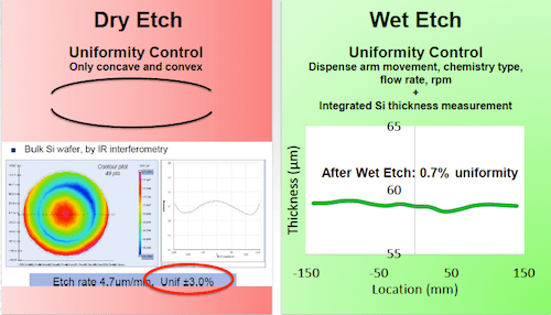
Wafer thinning to reveal the Cu TSV contacts is a multi-step process that begins with grinding the device wafer, which has been temporarily bonded to a wafer carrier, to 5-10µm above the TSV. The goal is to use etch processes to remove the remaining silicon to achieve a 50µm thinned wafer with exposed TSV Cu contacts. After the grinding process, it is important to remove rough surface defects. If you use plasma, explained Mauer, this smoothing is done using chemical mechanical planarization (CMP) or dry polish, which is a costly process. With wet etch, the need for CMP or dry polish is eliminated.
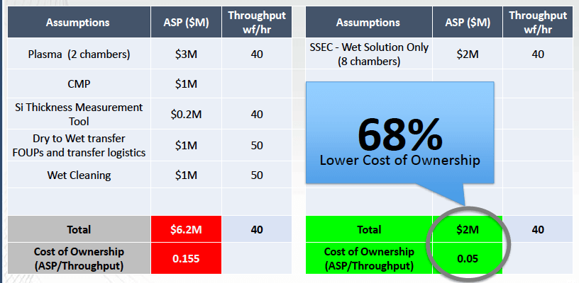
According to Le Roy, wet etch out-performs plasma etch in a number of critical areas including uniformity of the silicon etch process; elimination of surface roughness; and no temporary bonding material outgassing or damage to the bonding adhesive. It also offers improved oxide liner protection, with 10,000:1 selectivity to oxide vs. 180:1 of plasma process. Lastly, SSEC’s WaferEtch platform offers integrated Si thickness measurement used to determine an accurate endpoint of the TSVs across the entire wafer, and integrated cleaning; necessary steps that require dedicated tools in a dry process approach. SSEC’s value proposition for TSV reveal, says Le Roy, is that the company’s wet etch solution combines the capabilities of four separate tools required for the dry process reveal into one tool, for a 68% lower cost-of-ownership (Figure 1).
Based on demonstrations at customer sites, Le Roy says he is confidant that in terms of both CoO and performance, interest and awareness is growing for the wet etch advantage. He believes the reason for the initial adoption of dry etch processes in R&D centers is due to the availability of legacy dry etch tools, and that once the advantages are clearly understood, there will be a switch. All dry processes still ultimately need wet processes; after dry etch, residue still needs to be cleaned using a wet process. “Dry will not be our main competitor,” he predicts, “because wet is cheaper and has better uniformity control capabilities.” The competition, therefore, will be other wet wafer processing companies.
The Tour
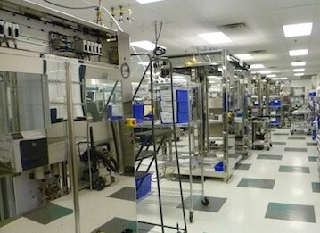
So what sets SSEC apart from other wet wafer processing tool suppliers? The answer to that question came from our tours of the manufacturing clean room and associated analytics lab, as well as the manufacturing floor where tools are assembled.

Itzkowitz explained that SSEC’s overarching philosophy is that each custom-configured tool starts with the process. SSEC’s development laboratory includes a full suite of its 3300 Series tools with all process capabilities, as well as the latest WaferStorm and WaferEtch platforms. The lab includes a complete line of metrology equipment to provide rapid feedback and speedy optimization of all processes. This is where Mauer’s team works with customers, running processes in the lab before designing the tool to their specification.
For example, the TSV Revealer is a custom-configured version of the company’s WaferEtch platform that includes integrated metrology for end-point detection. Mauer explained that her team has found that it’s not efficient to measure remaining silicon thickness (RST) because of the time it takes and the accuracy required. Thus, they have focused efforts to meet market requirements using integrated metrology to determine silicon thickness.
In this approach, integrated metrology sensors determine the exact amount of silicon thickness after grind, and the customer provides the TSV depth. TSV depth is then subtracted from the total silicon thickness, and wet etch is performed using a time-based method. The TSV Revealer also offers more parameters to control the etch process across the wafer thanks to the hyperbolic control arm movement, which can be adjusted to deliver a uniform etch result (Figure 2).
All of SSEC’s systems are built to order from standard assemblies, explained Itzkowitz. All electrical design and proprietary software is developed in-house. Another unique feature is that each robot and chamber is equipped with a camera that handles, registers, and aligns parts. “We record everything that goes on during a wafer process and save it for 30 days so that we can go back and reference if needed,” said Itzkowitz. He added that each machine is equipped with three networks: an Ethernet port for transmitting large amounts of data; RS422 for system control; and coordinated motion CAN.
SSEC tools are built to last and are backwards compatible. Itzkowitz noted that it is not unusual to be asked to provide support for a tool that was installed 20 years ago. “When we develop these machines we go one step further,” he said. “If a commercial component is weak, we’ll develop our own.” As an example, he pointed out a high-pressure pump they designed in-house because there wasn’t “a good one” available.
Another distinctive feature that sets them apart from other tool manufacturers is that the tool’s electronics are integrated into the sub-assemblies; which eliminates the need for a separate rack to house the system’s electronics. This makes the tools more compact and easier to manage, says Itzkowitz. It also makes them easier to build, test, and diagnose. He estimated that from order intake to tool install takes 16 weeks. Average selling price of an SSEC tool is 1$M, and ranges from 400K -2.5M depending on the required throughput and process custom configuration, which affects the number of chambers required.
As we wrapped up the visit, I left with a new appreciation for SSEC’s approach to tool manufacturing, and the performance and cost advantages its tools can bring to 2.5D and 3D IC manufacturing. I expect to be hearing a lot more from them as 2.5D and 3D IC approach volume manufacturing. ~ F.v.T.


