

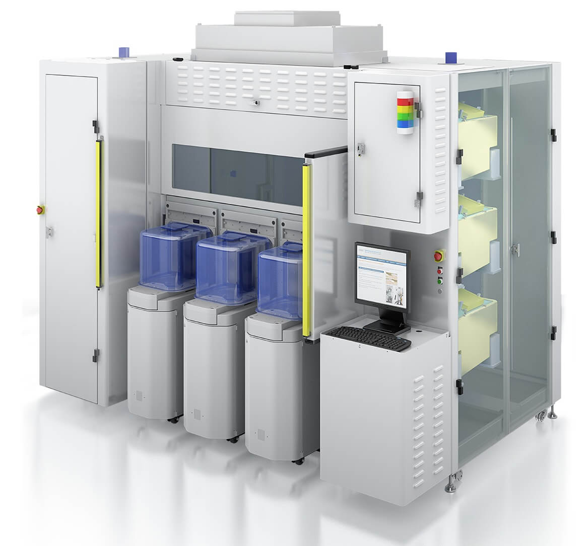
 SSEC’s WaferEtch™ TSV Revealer is a single wafer wet processing platform for 3D IC and interposer wet etching applications designed to reduce processing and capital equipment costs. The WaferEtch features superior uniformity of silicon thickness (as low as -/+ 0.7%).
Testimonial
Via reveal is a critical process step in 2.5D and 3D IC technologies that involves thinning the backside of the wafer to reveal the copper interconnects. This has become a focus area for 2.5D and 3D IC manufacturing to improve process control and reduce costs. SSEC’s WaferEtch™ TSV Revealer addresses these targets as a low-cost wet etch process with integrated metrology for performing thickness measurement and end point detection. The TSV Revealer replaces four tools required for dry etch process including: CMP, plasma etch, clean, and silicon thickness measurement. This achieves a significant reduction in CoO making 3D TSVs more economically feasible.
With the WaferEtch platform, it is estimated that the CoO is 68% less when compared to the dry etch process. The higher throughput and decreased capital equipment cost enabled by the WaferEtch means lower overall development and production costs, helping to bring 3D ICs to high volume manufacturing.
SSEC Website
Date this Product was Introduced to the market: 7/8/2013
Category Product is being Nominated for: 3D Manufacturing Equipment
Technical Information for WaferEtch TSV Revealer


