


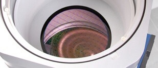
Nothing makes me click a link faster than a title like “3D Chip Stack Tool Sends TSV Into High-Volume”, because who in this industry isn’t waiting for that precise moment when through silicon vias (TSVs) go into high volume manufacturing? Unfortunately, the EE Times story behind that provocative title was a little less than accurate, because as we all know, one tool introduction isn’t going to send 3D TSVs into volume manufacturing! It’s going to take a bit more than that; like an order from a major device manufacturer. I decided to find out what the real story was, and as luck would have it, Isaac Ow, Global Product Manager, Metal Deposition Products, Applied Materials (AMAT), was also at ECTC 2014 last week. He was more than happy to brief me on the Endura Ventura, the company’s new physical vapor deposition (PVD) tool, and the first in the industry to be design specifically for metallization of TSVs in high volume manufacturing.
So you may be thinking, as I was, that there are a number of PVD tools already available for metallization of TSVs for 3D ICs in HVM. Oerlikon has one; SPTS has one; and Tel-NEXX has one, just to name a few. But the difference, according to Ow, is that these tools were designed for PVD for wafer level packaging (WLP) applications, not TSVs. “There have not been dedicated efforts for PVD technology to fill high-aspect ratio TSVs in the production environment,” explained Ow. “What exists are PVD tools targeting copper (Cu) pillar bumps.” And, he explained, therein lies the difference.
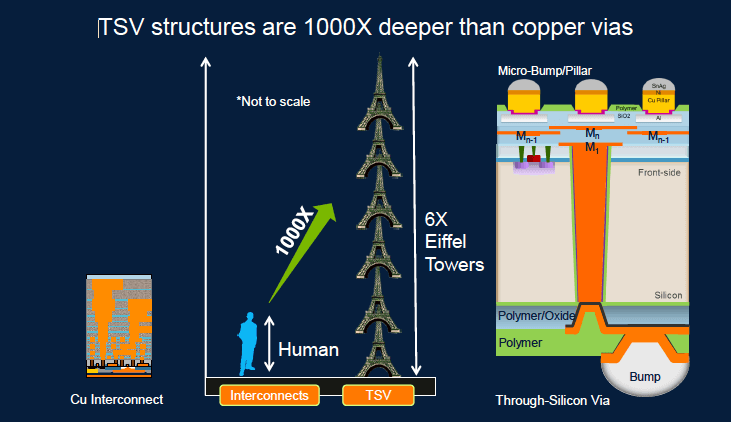
Ow said that for under bump metallization, Cu pillars, and bumps in WLP applications, standard PVD with blanked deposition is fine because there are no structures with coverage requirements. Not so in the Cu interconnect world, where PVD is designed to fill tiny structures. “We know how to get material to the right area,” said Ow. He demonstrated how AMAT has leveraged its expertise in existing Cu interconnect integration schemes, which can be mirrored in TSVs, but at a much larger scale. TSV structures are 1000x deeper than Cu vias used in front-end fabrication (Figure 1). The goal is to provide continuous barrier and seed layer coverage without gaps in hard-to-reach places. Additionally, front-end processes use tantalum (Ta) for the barrier layer, which is cost-prohibitive when adapted for TSVs. AMAT has come up with a system that integrates the much less costly option of titanium (Ti) as a barrier material, said Ow.
“Applied Materials has come in with front-end technology expertise, and has innovated and applied what we have to meet all advanced packaging requirements, which is changing from a technical perspective,” he said.
In the Endura Ventura PVD system, says Ow, directionality is improved due to an enhanced line-of-sight that efficiently deposits material in hard-to-reach corners. This has increased the gap fill window by 50%. As a result a thinner barrier seed can be used to achieve the same gap fill performance of interconnect PVD systems. The system integrates Ta, Ti, and Cu chambers to accommodate customer’s choice of materials. The Ventura chamber technology is enabled on Endura’s industry-proven mainframe, noted Ow.
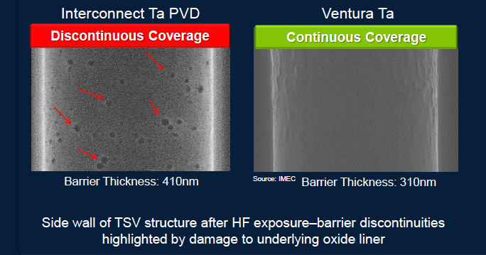
Ow showed me the results of a comparison study of the interconnect Ta PVD technology vs. the Ventura Ta PVD tool when used for TSVs (Figure 2). Samples processed in each tool were dipped in diluted Hydrofluoric (HF) acid. Holes in the Ta PVD sample indicated that HF attached to the underlying oxide, which means there was not enough continuous coverage of the barrier layer to protect the underlying Si. The sample from the Ventura TA PVD tool showed continuous coverage. Additionally, Ow said the standard PVD tool started with a thicker barrier layer – 410nm vs. 310nm – and the Ventura still performed better. Ultimately, Ow says the Ventura configured for Ta/Cu barrier/seed demonstrated 50% reduction in cost over existing PVD technologies, and when Ti is used instead of Ta, and additional 20% cost savings can be realized.

“The main barrier to HVM adoption of 3D TSV technologies is cost,” says Ow. “With the Ventura, we believe we are playing our part in mitigating this cost barrier.” Customers must agree, as the company has shipped 30 Ventura chambers in the past 18 months.
So there you have it. While AMAT’s Endura Ventura isn’t necessarily taking 3D TSVs into volume production all by itself, the tool’s existence just might help bring us a few steps closer. ~ F.v.T.


