


This year’s IMAPS International Symposium purported to have “the most interposer and 3D content under one roof.” I’m not sure about that, but there was certainly enough 3D going on at IMAPS 2014 to spark my interest. Here are some highlights I came away with, based on presentations, interviews with industry suppliers and a stroll around the exhibitor floor.
The Glass is Half-Full
As Venky Sundaram, 3D Systems Packaging Research Center, Georgia Tech, pointed out, four years ago he was the only presenter talking about glass interposer technology. This year there was an entire session dedicated to glass interposers, and a total of 7 papers presented (one in a separate session). The topic titles ranged from general — “Glass Substrates for Advanced Packaging,” and Low-cost Glass Interposer Development” — to highly specific — “High Reliability and High Performance 30um Through-Package-Vias in Ultra-Thin Bare Glass Interposers”, and demonstrated a push for the glass interposer market.
Sundaram’s presentation reported favorable results on the thermo-mechanical reliability and electrical performance of 30µm through package vias (TPV) formed on ultra-thin, un-coated glass interposers metallized using Cu sputter and electroplating processes.
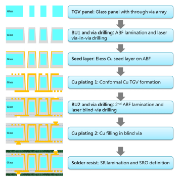
Yu-Hua Chen, Unimicron Technology Corp., reported that the company has successfully demonstrated fabrication of glass interposer daisy chain test vehicles using 508mm x 508mm glass panels on a high volume manufacturing (HVM) substrate line (Figure 1). The through glass vias (TGVs) are laser-drilled, and a Cu seed layer is deposited via conformal plating. Chen said the four-layer glass core exhibits 3x better flatness than organic cores, with less than 50µm warpage, as well as achieves fine line and spacing of 8/8µm, and expects to achieve future line/spacing of 3/3µm. “This shows significant promise for continuing to explore and develop glass as a new substrate material,” said Chen.
However, singulation of panelized glass interposers still poses major reliability issue. Sundaram said the Silicon and Glass Interposer Consortium at the 3D Systems Packaging Research Center is working 10 different singulation methods to come up with a solution to this problem. They are working on optimized mechanical blade dicing with Disco that involves post-treatment of the glass. Laser-based technologies will require infrastructure changes. “We’ve got promising data on singulated samples,” noted Sundaram. “There are lots of suppliers working on this.”
Ditch the Temporary Carrier
At past conferences this year, it has been suggested that the way to solve the temporary bond/debond challenge for 3D IC manufacturing is to ditch the carrier altogether and find an alternative approach.
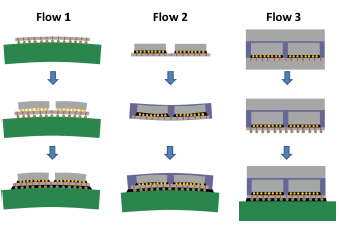
One of the key points in a presentation by Liang (Frank) Wang, Invensas, on assembly and scaling challenges for interposer technology, was a way to do just that by replacing the temporary carrier with a permanent one. This processes avoids the temporary bond/debond, and wafer handling steps, while also avoiding warpage and providing good co-planarity.
Wang explain that in this flow, bumped die are first attached to a full-size interposer wafer with unrevealed TSVs, and then bonded and underfilled. Next, a permanent support wafer is attached to the top of the bumped die, and the interposer wafer goes he through the thinning, reveal, patterning, RDL and bumping steps. Lastly, the full stack including the support wafer is singulated and the die stacks are attached to the package substrate using flip chip processes.
Wang explained there are limitations to this process flow if the total die thickness needs to be very thin. “The total package thickness varies based on the thicknesses of the die, interposer and carrier,” he said. “In most with 2.5D, it can meet most thickness requirements. For ‘true’ 3D, it’s a different story and depends on the application.”
Additionally, this process flow does not allow for the interposer and die to be manufactured completely in parallel. While the front-side processes on the interposer can be completed, the backside processes have to wait until top die are available. It is still however, a lower cost option due to the elimination of the temporary bond/debond steps.
Another approach targeted at managing warpage that Wang addressed involved fine pitch micro-bond bumps with low standoff. Fine-pitch bumps reduce the amount of solder needed. If you reduce the amount of solder, the bumps bridge each other less. Solder can compensate for coplanarity. “If you can solve this, you can manage warpage from the very beginning,” said Wang.

Modeling for Refinement
I also had a chance to speak with Rudolph Technologies’ Jim Webb, who was awarded Best in Session for his paper titled “Comparison of Measured and Modeled Lithographic Process Capabilities for 2.5D and 3D Applications Using a Step and Repeat Camera”. Webb’s paper focused on work done in collaboration with GenISys, a company that develops software for resist modeling, to understand the limits of current step-and-repeat lithography optics for advanced packaging applications, and to understand the roadmap for the future.
By inputting resist parameters into the GenISys software and comparing the resulting models with actual SEM images, necessary adjustments can be determined. Once the model matches the desired SEM images, process changes can be made to the tool to adapt it to achieve the desired results. “It’s easier to do this on a model than an actual test vehicle,” said Webb.
The model aids in identifying issues and finding solutions. It also allows you to see if you’re within the control conditons. One way Rudolph is using it is to qualify optics from the supplier and refine them. The software can also be used to qualify a specific resist for use in a particular application and support and validate results.
“We will continue to work with the resist modeling company to refine software to best represent thick resist behaviors, so that we can use it to understand limitations of current technology capability and look at roadmap for future needs,” said Webb.
Progress in High Aspect Ratio TSVs
Tango Systems had some interesting news to share regarding its PVD capabilities for high aspect ratio TSVs. Conformal coverage of TSV sidewalls and bottom in seed layer deposition has been a particular challenge for high aspect ratio (HAR) TSVs.
“We’ve recently proven we can get conformal coverage on up to 15:1 HAR TSVs,” said Zal Dordi, product manager for Tango Systems. As the industry trend moves toward growing via aspect ratios for improved performance, this will become a critical capability of PVD tools and processes.
Dordi noted that this achievement involved overcoming such challenges as good coverage on the bottom including the corners, and continuous sidewall coverage. This is a critical step in plating. “We’ve spent time over the last few years fine tuning hardware and process conditions to develop a new TSV platform based on our existing tool,” said Dordi.
Overall, while it may not have been the most 3D content under one roof when compared to the other 3D focused events, this year’s conference offered more interposer and 3D related than it ever has before, and the number of exhibitors who classify themselves as 3D IC and Packaging Technologies, TSV, and TGV reached 27. Not bad for a show known to focus on classical packaging technologies! ~ F.v.T.


