
While GLOBALFOUNDRIES and STATS ChipPAC may have it all figured out, there are many who still consider temporary bond/debond (TB/DB) to be an unsolvable challenge that adds unnecessary cost. The solution? Find a way to do away with it altogether. During the 3D IC Forum at SEMICON Singapore, both A*STAR Institute for Microelectronics (IME) and Invensas Technologies demonstrated that the best way over this particular wall is to just blast through it.
In his presentation, Manufacturability considerations in 2.5D, Sitaram Arkalgud, director of the 3D program at Invensas Technologies, revisited his technology score card, and has narrowed the choke points to two: TB/DB and backside low temperature oxide bonding. Temporary bonding is a process that doesn’t show up in the end product, yet adds complexity and temperature restrictions to what you can do in backside processes. He explained that being restricted to low-temperature backside processes could result in inferior quality of parts with reliability problems and irreversible warpage changes caused during thermal cycling.
Arkalgud talked about a decade of struggle with this particular issue that began during his tenure as director of the 3D enablement center at SEMATECH. “Temporary bond/debond adds a lot of process steps with lots of headaches,” he said. “We’ve been working on this for ten years, and the situation has not changed. It adds to the overhead costs. What we need is an approach that eliminates temporary bond/debond and allows scaling of the wafer thickness.”
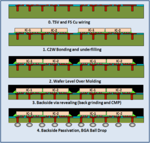
He cited two such approaches in the market; one involves die placement on an interposer followed by compression molding. The mold compound provides the stability while the backside processing is done. Both Invensas and IME have developed process flows based on this concept (Figure 1). Another carrier-less approach is Tezzaron’s FaSTACK, in which wafers are aligned, bonded, and diced apart.
Arkalgud described three process flow approaches for die-to-interposer attach. In the first, the thinned interposer is first attached to the package substrate. Micro-bumped die are then attached to the interposer and underfilled. In the second flow, µbumped die are attached to a thin interposer block, and then diced and mounted on the substrate. In the third flow, dies are attached to a full thickness interposer and then compression molded. This allows for backside processing without a carrier. This third flow gets away from TB/DB, thin wafer handling, and warpage control. “I believe this is eventually the way to go.” said Arkalgud.
He concluded by saying that non-recurring engineering (NRE) will be an important factor for <20nm lithography shrinks, and that large interposers will be expensive. “We should consider adding more functionality to large interposers, and using smaller interposers for cost-sensitive applications,” he said. “Assembly alternatives must be evaluated for lower cost, and smaller microbump pitches and shorter TSVs will need scalable thin wafer handling techniques.”
Surya Bhattacharya, Ph.D. of A*STAR Institute of Microelectronics concurred with Arkalgud on both the need for carrier-less wafer handling, and on the need for both cost-efficient active interposers and low-cost passive interposer solutions to address the variety of market needs. “Volume is definitely impacted by cost, and low cost is a critical requirement for mobile, CPU/GPU, and game console systems needing Logic and Memory integration,” explained Bhattacharya. As such, the research center has focused efforts on developing processes to suit different I/O densities and cost points.
At IME, his team has developed a low-cost 2.5D interposer platform that uses an approach similar to chip-to-wafer with over-mold as carrier – resulting in a carrier-less approach to avoid TB/DB. Additionally, they’ve replaced the costly front-side damascene Cu with plated RDL along with low cost polymer build-up process. Part of the challenge with this was achieving <5µm line and space. After extensive collaboration with materials developers to perform reliability assessments on different low-temperature cured photo-dielectric materials, Bhattacharya reports achieving 4µm pitch RDL i.e 2µm line and space.

In addition to the low-cost 2.5D interposer platform, IME’s suite of offerings includes an active through Si interposer (TSI) technology featuring photonic integration on the interposer for data center applications. This can be a cost-effective solution for this particular function, he explained, but is not to be confused with low cost.
The active (smart) TSI has elements such as an RF/Analog, repeaters, I/O, and ESD protection built-in, to add value and make it more cost effective. A via-last approach from the backside provides a modular, and therefore OSAT compatible, approach for system scaling.

Lastly, the research center is offering a high-density fan-out WLP technology for mobile applications. There are no TSVs involved in this technology, but to achieve high density and avoid die shift issues of traditional FOWLP approaches, they are adopting an RDL-first approach (vs. traditional mold-first) that eliminates die-shift issues and allows for scaling well below 5µm line and space – the current limit for FOWLP technology. This work is the focus of a new high-density FOWLP Consortium just launched in April 2014.
As previously mentioned, IME’s goal is to provide a suite of options for customers. “Which technology gets used is based on I/O density and line/space requirements of the target application.” explained Bhattacharya. TSI active interposer target I/O counts of 5000-10000. Low-cost passive 2.5D interposer targets between 2000 and 5000 I/Os. RDL-first, high density FOWLP targets less than 2500 package I/Os. As future technologies will continue to have unique requirements, a one-size-fits all approach will not be the way to go. Options will be the name of the game. ~ F.v.T.


I wonder why the concept of Disco’s Taiko wafer is discussed that little or not at all since it is a concept that is already in production with power-semiconductors. And why there is little discussion about changes that could be applied to the (handling-)equipment to help overcoming the need for rigid substrates. I think a lot can be done there instead of taking recurring costs for TB/DB etc…
Hi Sven,
The first time I ever heard the Taiko process mentioned was in December, 2013 at the 3D ASIP Conference. Dave Howard, TowerJazz Semiconductor gave a presentation. I talked about it here (end of the post) https://www.3dincites.com/2013/12/3dasip-2013-jan-vardamans-3d-readiness-report-card/. Currently its being used on 200mm wafers. I too was curious about why this was the first we were hearing about it. I would be interested in learning more about how it works for interposer and 3D IC applications on 300mm wafers.
I think it would be hard to apply TAIKO to TSV application because it is more thinner and much more process like etch, PECVD, CMP even with all bumping process should be applied. surely Taiko would be good solution at handling for PWR device but not for TSV.
Also, in technical things, wafer edge ring(edge bone) is a barrier to process in all following backside process. it means that all equipment should be modified, which is much bigger cost adder.