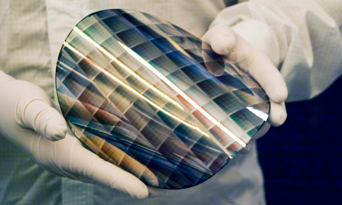
Fan-out wafer-level packaging (FOWLP) is a cost-effective way to achieve high interconnect density and to manage larger I/O counts within an affordable package. It enables smaller footprints, higher interconnect density, better routing and thinner packages than current technologies. [1] A standard FOWLP wafer comprises known good die (KGD) and a redistribution layer (RDL) or layers embedded in mold compound, which reduces the production of devices with defects, and provides more flexibility in 2.5D and 3D integration design. FOWLP process flows fall into two categories: chip-first and chip-last, referring to the point in the process when chips are placed onto the substrate. Chip-first processing has existed for a few years and is currently used in large-scale production. Chip-last processing, also called RDL-first, is still in early development.
A variety of process flows have been developed to meet flexible design requirements for a chip-first approach (Figure 1A). [2,3] In general, KGD are placed on a substrate that has been laminated onto a removable tape. Mold compound material is then layered over the KGD and cured. The substrate is subsequently separated from the lamination tape, followed by RDL buildup and solder-ball attachment. In the last step, the wafer is singulated for future processing.
Wafer-handling challenges can occur after molding, because the high-temperature processing used during RDL processes to crosslink dielectric materials can introduce stress that leads to warpage, due to the coefficient of thermal expansion (CTE) mismatch between Si and the mold compound.
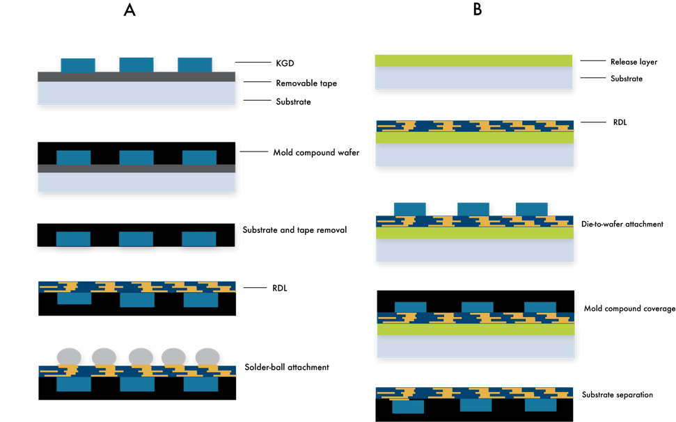
In a chip-last approach, RDL layers are built up on a carrier wafer. Then, KGDs are attached to the well-structured RDL followed by over-mold, curing and solder-ball attachment steps. Every step of the process is novel and therefore inherently challenging.
In both chip-first and chip-last processing, device wafers are temporarily bonded to carrier wafers using a specially formulated material applied at an elevated temperature to achieve the desired melt viscosity. During the debonding step, both the carrier wafer and attached temporary bonding material are removed from the device wafer using one of four main debonding techniques: chemical, slide, mechanical, or laser debond. Each technique targets specific applications.
During chemical debond, the bonded wafer pairs are immersed in solvents to dissolve the temporary bonding material. Because only the edges of the bonded pairs are exposed to solvent, this is a time-consuming process that adds to processing costs. In slide debond, the bonded wafer pairs are heated until the material softens enough to flow, and then the device wafer is separated from the carrier wafer using horizontal force.[4] For slide debond to be effective, the Tg of the temporary bonding material can neither be too high nor too low. More advanced technologies use a release layer between the bonding layer and the carrier or device wafer to enable either mechanical or laser debond.[5]
Chip-First Processing
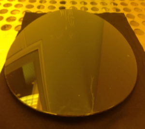
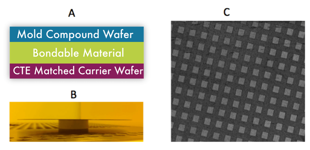
Wafer warpage due to high-temperature processing is the biggest challenge in chip-first processing. Warped wafers cause misalignment and are difficult to pick up. Figure 2 shows a mold compound device wafer bonded to a rigid thin glass carrier wafer using an epoxy-based temporary bonding material that warped after undergoing thermal simulation at 250°C for one hour. This could be due to the CTE mismatch between the mold compound, bonding material, and carrier wafer. Fortunately, the problem can be solved using specially selected temporary bonding materials (Table 1).
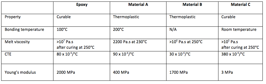
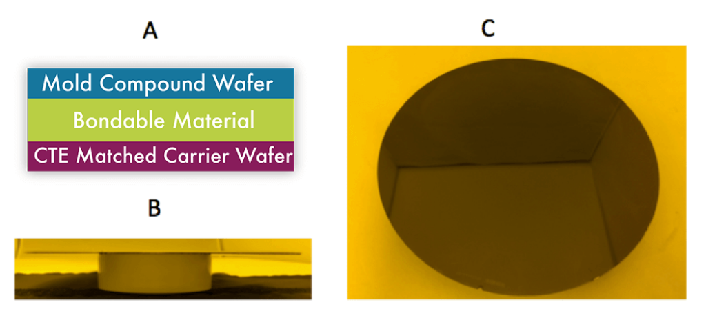
Figures 3 and 4 below demonstrate a successful example of decreased warpage. A temporary bonding material and a carrier that more closely match the CTE of the device wafer reduce the severity of warpage. In this process, a mechanical release layer was first coated onto the glass carrier wafer before spin coating with Material A (Table 1). After bonding the carrier to the reconstituted device wafer at 200°C, a thermal simulation of 230°C was applied, the pair was debonded using slight mechanical force, and the device wafer was cleaned with organic solvents.
The bonded wafer pair did not demonstrate warpage after thermal simulation, which can be attributed to the CTE match between the device and carrier wafer, as well as Young’s modulus of Material A. Young’s modulus represents the hardness of the material, which impacts wafer stress during the heating and cooling processes. A soft material with low Young’s modulus generates low warpage, while a hard material with high Young’s modulus generates high warpage.
In this case, regardless of the CTE mismatch between the mold compound wafer (6-20×10-6/°C) and Material A (90 x 106/°C), the relatively low Young’s modulus of Material A (400 MPa) ensures that the bonded pair successfully passes thermal simulation. Thus, the failure to pass processing shown in Figure 2 above can be attributed to the high Young’s modulus of the epoxy-based bonding material (2000 MPa).
When a CTE-matched carrier wafer is not available, using a material set that can be bonded at room temperature and cured at low temperature is successful at avoiding wafer warpage. In this example, a release layer (Material B) is spin-coated on the reconstituted device wafer, while a thick layer of low-temperature curable Material C is applied to the carrier wafer, and subsequently bonded. After thermal simulation at 250°C for one hour, the bonded wafer pair did not show any voids, delamination or observable warpage. The high melt viscosity of both protective Material B and curable Material C ensures adequate mechanical strength at high temperature. Moreover, the low Young’s modulus of curable Material C (3 MPa) does not introduce further stress to the bonded wafer pair. After successful thermal simulation, the bonded wafer can be either mechanically debonded or laser debonded, and the protective Material B can be cleaned by an organic solvent.
Chip-Last Processing
In a chip-last approach, RDL layers should be built upon a substrate that has a removable support layer, which is needed for downstream release purposes and that acts as the foundation for the entire wafer build up. In traditional RDL processing, a copper seed layer is deposited on the substrate via chemical vapor deposition (CVD).

In chip-last processes, the copper layer can pose a challenge, as the removable layers must withstand both the temperature and vacuum that are applied during the CVD process. Additionally, excellent adhesion between the removable layer and RDL seed layer is mandatory.
Figure 5 shows the comparison of copper deposition on laser-release materials, which either exhibit poor adhesion or good adhesion to the seed layer. In the case of poor adhesion, the surface of the laser release material showed bubbles after copper deposition, and the copper coating could be easily peeled off. With good adhesion, the laser-release material allowed for a smooth and strong copper coating, which facilitated support during subsequent processing.
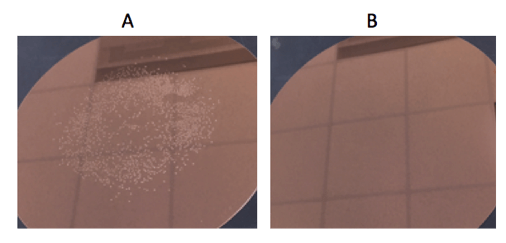

Figure 6 shows a more convenient method for applying the RDL seed layer than CVD. The removable material was first coated on a silicon substrate and then a thin copper foil was laminated at elevated temperature, resulting in a defect-free copper seed layer. The lamination process is cost-effective and suitable for large substrates such as panels.
As with chip-first, high temperatures are required during dielectric cure, die-to-wafer attachment, and mold-compound curing. These high-temperature processes pose new challenges for a removable material requiring high melt viscosity because it must have adequate mechanical properties at elevated temperatures to provide the necessary alignment.
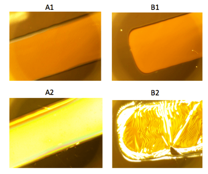
Figure 7 (A) shows a copper layer deposited on top of a high-Tg material that exhibited no surface changes after thermal simulation. When the copper layer was deposited onto a low-Tg material, as shown in Figure 7 (B), wrinkles were observed after thermal simulation. These wrinkles will prevent further device processing; thus, high-Tg materials may have more advantages than low-Tg materials.
Conclusions
Clearly, there are inherent challenges to both chip-first and chip-last FOWLP processes. Brewer Science has devised some options to surmount these challenges, such as bonding materials that demonstrate low Young’s modulus. Brewer Science also provides innovatively designed release materials that offer sufficient mechanical strength to bond successfully to the temporary bonding material, while also maintaining integrity during the entire process. With these in hand, manufacturers can successfully make their first forays into this new and exciting technology arena.
Acknowledgments
We acknowledge Nanium for providing test wafers; Industrial Technology Research Institute of Taiwan for copper deposition; and Brian Sandusky and Deborah Blumenshine for the copper lamination work.
References
- Bezuk, Steve. “Applications Drive Packaging Challenges in Growth Markets.” ConFab Conference, 2014.
- Fan, Xuejun. “Wafer level packaging (WLP): fan-in, fan-out and three-dimensional integration.” Thermal, Mechanical & Multi-Physics Simulation, and Experiments in Microelectronics and Microsystems (EuroSimE). 11th International Conference on IEEE, 2010.
- Fan, Xuejun, and Qiang Han. “Design and Reliability in Wafer Level Packaging.” Electronics Packaging Technology Conference. 10th IEEE, 2008.
- Hermanowski, James. “Thin Wafer Handling: Study of Temporary Wafer Bonding Materials and Processes.” 3D System Integration. IEEE International Conference on IEEE, 2009.
- Liu, Xiao et al. “Temporary Wafer Bonding Materials with Mechanical and Laser Debonding Technologies for Semiconductor Device Processing.” International Symposium on Microelectronics. Fall 2016. No. 1. International Microelectronics Assembly and Packaging Society, 2016.
Authors
Qi Wu, Xiao Liu, Kuo Han, Dongshun Bai, and Tony Flaim, Brewer Science, Inc.