
Continuing our look at presentations at the 2020 IWLPC, one of the themes of the conference was panel level processing.
Canon
Doug Shelton of Canon discussed “Submicron Lithography Enabling Panel Based Heterogeneous Integration”. While panel level processing (PLP) is efficient for large packages, processing equipment changes are required to process large panels.
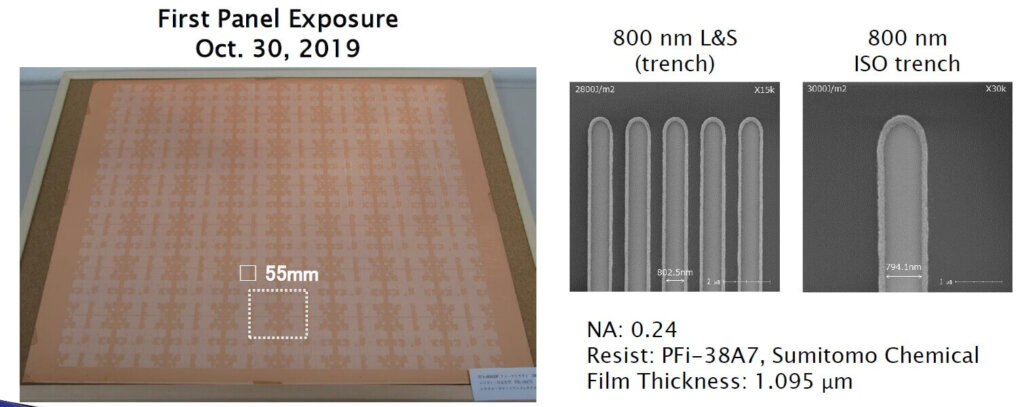
Uniform panel coating is required for submicron lithography (i.e. 1µm resolution processes require +/1 2% coating uniformity). Spin coating is not a preferred deposition technique for large panels due to the difficulty in spinning rectangular structures and the resultant poor coating quality at corners. Therefore, panel coating tends to use a slit coating process. Cannon and its equipment partners have been able to achieve <2% photoresist uniformity with selected slit coating tools. Using their FPA 8000iW panel stepped they have achieved 800nm L/S as shown below. Panel CD uniformity is <2%.
TOWA
Towa-USA presented “Fan-out WLP Advanced Manufacturing Solution for fan-out WLP/PLP by DFD (Die Face Down) Compression Molding”. Towa says it invented and commercialized compression molding in the early 2000s to compete with the standard transfer molding process.
SEMI adopted a standard for PLP panel sizes in July 2019 (SEMI 3D20-0719: Specification for Panel Characteristics for PLP Applications). The specified panel sizes are 510 ±1.0 mm × 515 ±1.0 mm and 600 ±1.0 mm × 600 ±1.0 mm. Towa has developed compression molding technology as a technique suitable for large-format molding.
As in conventional transfer molding, the compression mold is composed of a preheated upper and a lower section. The granular or liquid resin is fed into the lower mold. To avoid air pockets vacuum technology is used to purge the air, which makes it possible to mold without voids. After this vacuum process, the resin is sealed by the immersion of the object set in the upper mold into the lower mold.
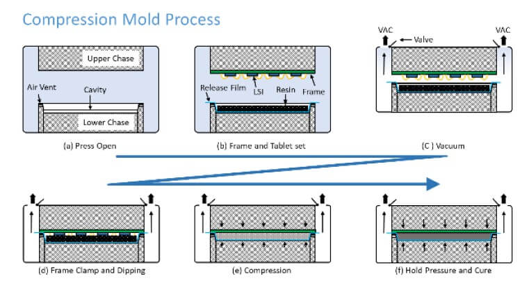
The larger the panel size, the larger the press size. The larger the press, the more difficult it becomes to achieve precision. The following are three approaches to this problem:
- The design concept of the press
- The flatness adjustment mechanism
- The resin supply method
As the products removed from the press after molding are not completely cured, they emit reaction gas, and if they are transferred to the next process without post-mold cure (PMC) defects may occur due to the reaction gas evolution. To eliminate as much as possible the difference in thermal history between products without a sudden change in temperature, an in-line oven unit is installed to stabilize warping variation.
Deca/Mentor
Deca and Mentor discussed the “Physical Level Verification of Panel Level Processing Designs Utilizing Adaptive Patterning Technology”.
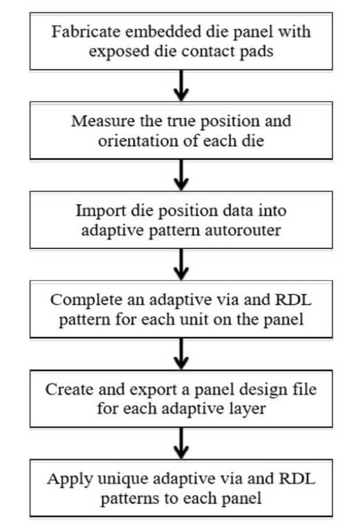
PLP of FOWLP suffers from die shift during the molding process. Adaptive patterning recompensates package design in real-time to compensate for die shift. The process sequence is shown in Figure 3.

To support the adaptive patterning flow, physical verification must be performed on the entire panel GDSII. Utilizing binning, multithreading and hyperscaling enabled the design team to successfully run DRC of the full panel in a reasonable time.
EV Group
EV Group presented “Maskless Lithography Optimized for Heterogeneous and Chiplet Integration”
Individual chiplets I/O bumps and interconnects pitch scaling nowadays moves towards 2/2μm L/S. Although the re-integration of larger dies from smaller chiplets, from various technology nodes, has shown numerous advantages over monolithic SoC technologies, this approach shifts the complexity into the integration and with it into the lithographic patterning processes.
The given reticle size and optics dimensions of static exposure systems limit the exposure area. This situation can become particularly challenging for larger area interposer fabrication, where stitch lines in the reticle stitch region can affect electrical properties within the redistribution layer (RDL). The ability to generate a stitch-less pattern for interposers exceeding current reticle size is increasingly important for advanced devices needed for complex layouts, such as in advanced graphics processing, AI, and high-performance computing (HPC).
Digital lithography is foreseen as a promising approach for tackling the above described challenges where traditional mask-based systems are reaching their limits. Since this method is maskless – fully digitally driven, it allows a very high degree of flexibility and therefore not only a rapid but in the long-term also a cost-effective solution for microfabrication.
EV Group evaluates common advanced packaging high resolution, thin and thick resists for RDL & μ-bump/μ-pillar manufacturing, utilizing maskless exposure to demonstrate its patterning performance. They conclude that maskless exposure technology provides a new approach for patterning comparing to the current lithographic techniques.
For all the latest in Advanced Packaging stay linked to IFTLE………………………..


