
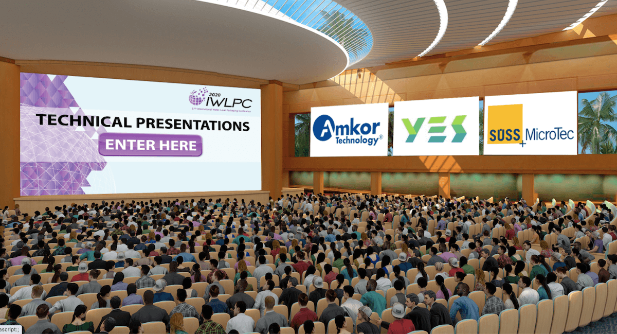
The 2020 International Wafer Level Packaging Conference (Virtual IWLPC) brought up the caboose of several weeks of virtual conferences that for me started with SEMICON Taiwan and included IMAPS International Symposium. The content featured one keynote, a panel discussion, 40 technical presentations, and 23 virtual exhibits where you can access still videos and product information about the companies. I was most interested in attending the live presentations and visiting the exhibitors during the live days, October 13-14, 2020.

Dan Oh, Samsung Electronics, set the stage by talking about his experiences at Intel, where he worked on EMIB, which he said required chip and package co-design. Intel is where Oh said realized the advantages of through-silicon vias (TSVs) and fan-out wafer-level packaging (FOWLP)
He took his experience with him to Samsung, where he helped build the 2.5D and panel-level packaging (PLP) infrastructure.
“15 years ago, shrinking would stop not because of technology, but because of cost. That was based on the cost of FPGAs,” explained Oh. That sentiment has changed. Now, he says, how to package and how to integrate ICs is becoming more important than fabricating the wafer itself.
“TSVs allowed wafers to be used as a package substrate, and allowed 3D stacking of multiple dies,” he noted. “In the early days, integration was done to reduce the form factor, not to improve the performance.” How times have changed. 10 years ago, 3D stacking was used in limited applications, such as memory. Oh said now, we can expect more devices coming in consumer and 3D.
Diving into Samsung’s advanced packaging solution, Oh discussed his work on chip-first PLP for Chip first PLP for wearables and chip-on-wafer for CMOS image sensors. He outlined advanced packaging design challenges such as signal integrity, thermal integrity, and power integrity, and detailed Samsung’s approach. You can still catch the presentation here until October 30.
Update on Panel Level Packaging
The other live event I tried to attend was Jan Vardaman’s panel discussion, Meeting Future Advanced Packaging Challenges: What’s Next? Unfortunately, I and a bunch of other attendees had trouble logging in because there was a double registration step that I still don’t understand, so by the time tech support sorted it out and logged in, it was half over. Luckily there was still lots to hear.
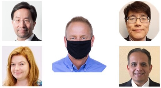
Panelists included Tim Olson, CEO Deca; Tanja Braun, Group Manager Assembly, and Encapsulation Technologies and Project Leader of Panel-Level Consortium, Fraunhofer IZM; Rahul Manepalli, Ph.D. Sr. Director of Engineering, SPTD & Sr. Principal Engineer, Intel Corporation; Max Min, Ph.D. Director, Package, and SI/PI Architect; Samsung FoundryShin-Puu Jeng, Ph.D. Director, TSMC.
The Question of Panel Size
I joined in just as Tanja was answering the question about standardization of panel sizes, to which she responded, “It’s already too late for standardization of panel size because so many different sizes already existing.”
The rest of the panel seems satisfied to settle on two standards: Intel is using 510 x 515, and Deca (nepes and ASE) use 600 x 600. Braun said the first FOUP systems for these dimensions are available from Japan, and volumes are ready to be shipped.
Min said Samsung would like to standardize panel sizes to reduce cost. He noted that in general, panels allow for more units per panel than round wafers. Min also said the biggest challenge of achieving fine line/space on panels is during the lithography step, and that you run into isolation issues due to the size.
Manepalli noted that Intel has been using 510 x 515 because is the standard in the IC world, and by standardizing it allows for economies of scale for equipment manufacturers. He said the real challenge is achieving high-yielding high layer count substrates that require lithography, etching, plating, planarization, and dielectric materials. “Innovations are needed to drive innovations up,” he said.
Olson reiterated that 600 x 600 and 510 x 515 are both SEMI standards, and will probably become the de-facto standards. “There are FOUPs, there’s infrastructure because of the trailblazing work done by Intel, ASE, and nepes. It’s ready,” he said. He alluded to “some exciting things happening right now” with chiplets at Deca licensees with high-density integration on large module sizes that are achieving a 70% cost reduction.
“I’m confident that giving the market interest in high-density chiplets, it will come,” said Olson.
Intel believes the future has to be on large panels, which means fab technology will also need to come to large panels.
Material Challenges
Materials are another challenge, particularly polyimides for mold compounds, noted Manepalli. While it’s possible to create multi-size vias, we need chemistries that allow for good via fill regardless of the size of the via being plated, he noted.

Braun added that in working on 2µm and 1µm l/s, Fraunhofer is learning what needs to be optimized with regard to dielectric materials.
Olson chimed in, noting that via pitch is often overlooked and that it will become more important as it continues to shrink. Adaptive Patterning helps, particularly when aligning, for example, a 10µm copper stud on a 5µm via. with Adaptive patterning helps, can make a large contact on a small copper stud.
The panelists talked about embedded die in laminate, which has seen little adoption. Braun said there are European projects on high-density laminate approaches, and that there is a lot of potential for high-density embedding in PCBs. More PCB companies are moving into that business, she said.
Manepalli said at Intel, EMIB is volume production and is used to connect HBM to graphics dice, and FPGAs. “Applications are growing. The method of using localized bridges with very high density where you need it will catch on more than we think,” he said.
Glass as a Substrate
General consensus is that it is still being used mostly as a carrier. Braun noted some projects in photonics applications with glass embedded in PCBs for optical applications. Manepalli said glass has benefits, such as allowing for better registration, but it is limited in capability. He cited challenges with fine line/space patterning because glass can’t tolerate large scale undulations. Additionally, he said how to create through-hole vias is still not solved. (They should check out the work being done by Plan-Optik and Mosaic Microsystems.)
The Matter of Inspection
Min noted that critical areas need inspection as package sizes get bigger, and speed and efficiency are important. “A large chip could be as big as the reticle.” He said.
Olson described Deca’s integrated metrology process step to debunk problems. He says yield is the number one challenge when you’re dealing with multiple layers and a chips-first-face up fanout process like M-Series.
“In the short term, we have to do 100% inspection AOI to make sure we have good substrates,” he said. “We’re working with existing suppliers to enhance our capability.” He explained that Adaptive Patterning allows for perfect connections because they are able to feed real-time data for each panel so that the inspection tool can set up parameters and inspect based on a specific design.
Unfortunately, I have not had time to go back and view the full recorded version, although you can still catch it here.
My Virtual Event Score Card
As virtual platforms go, I had high hopes for the IWLPC event – the aesthetics were great. The virtual people in the virtual hall moved. The booth designs allowed for more branding options than some of the previous events. But when it came to the exhibitor experience, it was an epic failure. Presumably to protect exhibitor’s proprietary content, booth reps were blocked from visiting other booths. So, for 3D InCites as an exhibitor, we couldn’t take advantage of the text and video chat capabilities to visit our community member booths. When we did get visitors, I the chat function didn’t seem to be working. Other exhibitors I spoke with had the same issue and were frustrated by not being able to engage with attendees. In fact, the only way I was able to connect with other attendees was in the Tech Support chat room!
I would like to suggest to all organizations who are trying to generate revenue from virtual events that they either eliminate the exhibit hall altogether and just sell sponsorships to support great content, or up their game. Exhibitors are looking for a robust experience where they can engage and network seamlessly.
I’m told by one community member that the best virtual exhibitor experience they had as an exhibitor this year was Microtech Ventures’ Automotive LiDAR 2020, which was built on an AI-based networking platform. They have another event coming up, Medical Wearables 2020, built on the same one. You might want to check it out.
After I post this, I’m going on a much-needed vacation, hiking in Zion National Park where there is no WiFi. See you in November! ~ FvT


