

I have finally been in this industry long enough to understand the cycle of discussion, scrutiny, call to arms, and discussions that emerging technologies go through on their way to adoption. What I first witnessed with the building of the 3D IC ecosystem, is now happening with chiplets. This past week’s keynote talks and panel discussion at the 2020 IMAPS International Symposium put the emerging chiplet ecosystem through its paces – namely a call for standards, co-design tools, test solutions, thermal management solutions, and advancements in equipment and materials.
Intel Wants a Chiplet Ecosystem
Intel’s Babek Sabi kicked it off acknowledging what most of us have understood for some time: advanced packaging is the solution to replace system-on-chip (SoC) in terms of power, performance, area, and cost (PPAC).
“The shift to data-centric computing has created an explosion in advanced packaging,” he said. “We are at the tip of the iceberg of where we need to go with advanced packaging. Our (Intel’s) vision is to develop leading technology so that we can stitch together functionality to mimic monolithic SOC.”
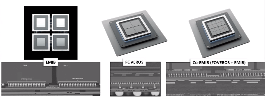
After providing the advantages of Intel’s offerings, namely EMIB, Foveros, Co-EMIB, and Omni-Directional Interconnect (still in the works and intended to extend 3D) (Figure 2), he described some challenges that must be addressed to fully support these technologies.
First of all, He reiterated that the fab, assembly and packaging worlds are converging, and that with all the functionality being packed into advanced wafer-level packages (WLP), the sizes of the packages are getting so large, that panel-level packaging is needed to make it affordable (Figure 3). (Those of you waiting for customer demand to shift to panel-level tools, take note).
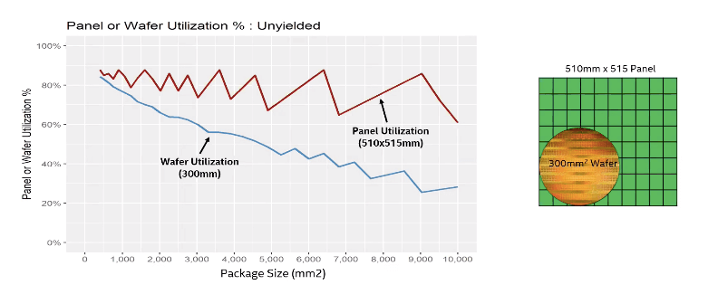
Figure 3: As die complexities grow, the economic cost advantage of manufacturing advanced packaging on panel vs. wafer will accelerate. (Courtesy of Intel)
Sabi also said that as hyper-scaled packaging becomes more fab-like, the industry is moving from laser technology to lithography to form vias that can scale to the required density. He called for silicon equipment providers to focus on developing tools that provide the capabilities to advanced packaging.
Other items on Sabi’s checklist:
- Standard die-to-die interfaces to simplify chip connection.
- Highly reliable dielectrics to support tighter bump pitches, particularly for 5G applications
- Advanced fab and assembly equipment to support Cu-Cu hybrid bonding, which will replace solder interconnects to achieve bump pitches of 20-25µm.
- Consider photonics as a replacement for copper interconnects in the future.
When asked whether Intel is ready to help with the investment of new fab lite processes, he said “It will pay for itself if we achieve really high-yielding substrates, so we can afford a more expensive infrastructure.”
In response to a question about the status of panel-level tools, he stated that vendors who had developed tools for 450mm processes and then had to abandon them are re-using the capabilities to develop panel tools, and multiple equipment providers are moving in that direction.
Regarding inspection technology to improve yields, he said better equipment is needed. (Interestingly enough, KLA just launched its next-generation suite.)
And lastly, when asked what the biggest challenge is with hybrid bonding, Babi cited cleanliness. “One small particle and the die is gone,” he said. “We need to have integrated, fab-like assembly tools where we keep everything clean.”
Bryan Black’s Chiplet Ecosystem
AMD Fellow, Bryan Black, has been an advocate of SoC disaggregation since he started spreading the message in 2014. The message then was that if we focus process nodes of specific functionality – diverse blocks of IP – we could end up with better cost per component. By allowing functionalities to scale at their own pace, his team at AMD determined they could reduce die sizes, improve yield, and get more die-per-wafer.
“Soft IP in RTO code is not as valuable as tested, yielding die to achieve the desired PPAC,” explained Black.
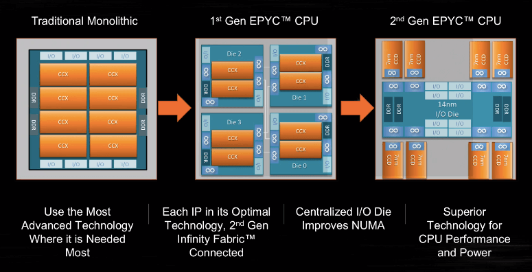
Based on this premise, AMD designed, built, and shipped its Fiji chip in 2015, the first graphic engine to use high bandwidth memory (HBM). He said this device kick-started an “aggressive trend in chiplets within AMD” most notably its first and second-generation EPYC processors.
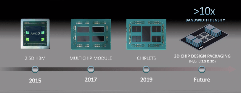
As of 2019, Black said the company is moving towards full 3D chip design solutions – not just stacked memory, but “stacked compute.” Why? He says chiplets enable more transistors at better yield; you only use 7nm and 5nm when that performance is needed; as silicon cost is reduced, you can shift to more expensive packaging solutions.
As a design house, Black said AMD is leveraging the engineering resources of foundries and OSATS to make this happen. “This allows us to build on our modular architecture strength and why we started building chiplets into our server platform,” he explained.
It’s not as simple as taking a monolithic die and splitting it in two. It must be done in a way that provides a straightforward solution. “Each time we partition a product, we look where we can reuse these devices,” he explained. “The goal is to create a chiplet library.” He agrees with Sabi, that industry standards will help, particularly where memory is concerned. “We need memory-consistent models, coherency, and virtual memory,” he noted.
Security is another issue: He said we need to determine where the security processor resides, which die is it on? How does it monitor other dies? How does it prevent denial insert?

Black also talked about what AMD calls “infinity fabric”, similar to what Subu Iyer refers to as “interconnect fabric” and TSMC calls “3D fabric.” These all go beyond what an interposer can achieve, explained Black. “Interposers are good at edge-to-edge interconnect, but not good at routing signals,” he said. This requires co-design between the package substrate and the silicon floorplan (Figure 5)
3D stacking chiplets exacerbates all the challenges of 2D, noted Black. We need to drive the TSV pitch to match the splitting/folding of the system. We need to redefine known good die (KGD) as ‘sufficiently good’, with a new test solution that can drive power delivery. He noted that bridge technologies (such as EMIB) are effective in managing connectivity between chiplets.
Overall, he seems impressed with the variety of fan-out and 3D stacking options for what he calls MCMs that are out there: “The diversity of options is incredible, and we think we’ll use them all in a single product.”
Is it an Ecosystem or a Village?
For her annual panel discussion, Jan Vardaman rounded up an impressive panel to discuss The Future Advanced Packaging Ecosystem: Who Will Be in the Driver’s Seat? And by advanced packaging ecosystem, she really meant “Chiplet Ecosystem”. This is where I had déjà vu back from when we were discussing the 3D ecosystem.
Panelists included Koushik Banerjee, Intel Corp.; Dan Berger, GLOBALFOUNDRIES; Eelco Bergman, ASE; Mike Kelly, Amkor Technology; Khai Nguyen, NVIDIA; Craig Orr, Samsung, and Ashkan Seyedi, Hewlett Packard Enterprises (HPE), providing representation from every possible “owner” of the chiplet architecture.
For once, the audience was not able to hijack the discussion, and the panelists had the opportunity not to just offer insight from each perspective, but to engage with each other to better understand the challenges and possible outcomes. All but Seyedi described what they saw as the role of the IDM, foundry, and OSAT.
Both Kelly and Bergman agreed that designs are driven by the developer and that while designs can be flexible, standard interfaces are going to be key.
Orr talked about the importance of design kits and reference flows. However, whoever has the technical capabilities to do this at scale and spread out the costs will be leading the charge. Until there are standards, all parts of the ecosystem need to be integrated, and foundries will have a role to play going forward.
Berger said he thought the foundry can play a significant role, but still requires the end customer and OSAT to play a leading role. He said IDMs won’t be able to hit cost points. “The flexibility and EDA standard that foundries are offering and driving could offer a lower-cost solution going forward,” he said.
Bannerjee, of course, disagreed with Berger, noting that while OSATS and foundries offer rich options, IDMs have specific advantages, such as being able to offer both product and foundry profit margin. “The decision lies with whoever owns the product. They need to pick what is best for their needs,” he said.
Nugyen noted that while the fabless design house owns the chip design liability, it is the foundry’s design kit that dictates the interconnect architecture. It’s all about the partnership between the supplier and the IDM, and the right operational conditions. But when it comes to device failure, it all comes down to whoever’s name is on the chip.
Bergman, however, sees it slightly differently: “When a failure does occur, it goes back to the village, at the end of the day,” he said. “The supplier is responsible for the product, but the supply base needs to support it and help identify the underlying problem.”
As an end-user customer, Seyedi did a great job of stirring the pot and voicing concerns on behalf of HPE.
“I think it’s (chiplets) interesting. But it’s nothing is new; we tried that 45 years ago and it didn’t work, and here we are again?” he said. “Let’s learn from what went wrong before. Why are chiplets important? Because no single entity has the knowledge to bring this all together. Not to throw cold water on this. But systems companies like one neck to choke when things go wrong.” Syedi added that when the optimization space explodes, it’s going to be tough to agree on standards because that’s like giving up the secret sauce.
The discussion about the need for a chiplet ecosystem that ensued provided the viewer with the feeling that they were a fly on the wall of a very intricate discussion – so much so that I really can’t do it justice by providing a play-by-play. If you have time to listen/watch to just one of the recorded sessions, it’s worth it just for this one presentation. Register here for full access to the on-demand program.
Stay tuned for more from IMAPS…


